Validating on-chip variation: Is your library’s LVF data correct?
Machine learning techniques help ensure the validity of Liberty Variation Format information for OCV analysis at lower process nodes.
The shift from 28nm to 20nm has been more awkward than usual for a number of reasons, many of them to do with the challenge of patterning 20nm features with 193nm lithography. This brings greater costs, increased process variability and therefore the need for more tightly coupled tools and more restrictive design rules.
The upshot is that although 20nm processes have been developed, they did not initially deliver the kind of ‘straightforward’ improvements in power, performance and area (PPA) that the industry has come to expect. Despite this, foundries such as TSMC and IDMs such as Intel are pressing ahead with 20nm.
Key customers such as Apple are rumoured to be committed to using them – despite the challenges – as are less well-known customers who are prepared to do the extra work necessary to get a worthwhile boost to PPA for their designs. With the cost to a fabless company of getting ready to design on a new process now reaching one to two billion dollars, though, it is not surprising that some have decided to move from 28nm planar processes directly to 14/16nm finFET processes.
In doing so, they have been able to benefit from the hard lessons learnt by the EDA vendors, fabless companies and foundries in making 20nm work at all, and then making it work well.
Antun Domic, senior vice president and general manager of the implementation group at Synopsys, said that the thing that is different in this transition is the extreme detail involved in applying the technology.
Mojy Chian, senior vice president, design enablement, GlobalFoundries, said that the 20nm node marked an inflection point in the foundry business that demands a level of collaboration between foundry and customers similar to that seen in an IDM.
Joe Sawicki, vice president and general manager of Mentor Graphics’ Design to Silicon division, focused on the variability issues of such dense processes.
Michael Buehler-Garcia, senior director of marketing for Calibre design solutions in the Design to Silicon division of Mentor Graphics, focused on the tools challenges of designing at 20nm.
Synopsys Fellow Tong Gao, focused on overcoming the physical challenges of 20nm design, especially the impact of double-patterning lithography on manufacturability, and routing to double-patterned cells without losing their density advantages.
The 20nm node brings number of specific challenges, including:
Early iterations of 20nm processes shocked the industry by costing the same or more per transistor than at 28nm – at least initially. Since new nodes have long delivered greater performance, lower power consumption and a lower cost per transistor, this was a wake-up call that was not well received in the industry. There are several reasons why 20nm processes are relatively costly:
In a presentation at IEDM 2013, Geoffery Yeap, Qualcomm’s vice president of technology, said that the costs of producing the back-end-of-line (BEOL) interconnect for mobile devices hit half the die cost in the initial 20nm processes, up from just over 40% at 28nm.
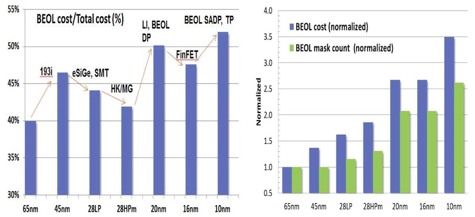
Figure 1 BEOL costs rose to more than half of die cost in the shift from 28nm to 20nm (Source: Yeap/IEDM)
At 20nm, the densest features on the critical layers of the process cannot be clearly patterned by a single mask illuminated with 193nm light. So called double-patterning lithography relieves interactions between dense features, but introduces extra cost for the critical layers, and adds another source of variability. This variability has to be modelled to ensure accurate parasitic extraction – otherwise, designers have to use such large guard bands that it undermines the advantages of the shift to 20nm. There are two main ways to achieve double patterning:
There’s a detailed insight into the impact of each approach on the variability of key process parameters by simulation company Coventor here.
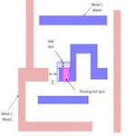
For the LELE approach, double patterning means finding ways to split critical features between the two masks. This has led to the development of mask-coloring algorithms, based on map-coloring algorithms, that can make the split without losing the design intent or introducing lithographic issues of their own. Support for these ‘colored’ layouts has demanded greater flexibility from tools in other parts of the design flow, such as place and route and layout verification, to handle double-patterned designs.
Figure 2 Placement tools have to ‘legalise’ designs by adjusting placement to meet double-patterning constraints (Source: Synopsys)
Analog and mixed-signal designers have been concerned about automated tools splitting critical polygons on their layouts, and so have asked for manual control of color assignment. And some foundries want to control coloring in-house, to meet their own lithography needs, while others have been happy to receive pre-colored layouts that do not necessarily reflect all the details of a particular process.
The density that is one of the main drivers for a shift to 20nm also brings with it the need to increase routing resources. The foundries’ response has been to introduce local interconnect (LI) layers – also called middle-of-line (MOL) layers – that offer a way to achieve very dense local routing below the first metal layer. Several of these layers may be available in a given process, and most don’t use contacts. Instead, they connect by shape overlap without needing a cut layer. Getting rid of contacts makes routing denser because contacts are bigger than nets, and can’t be placed too close to nets.
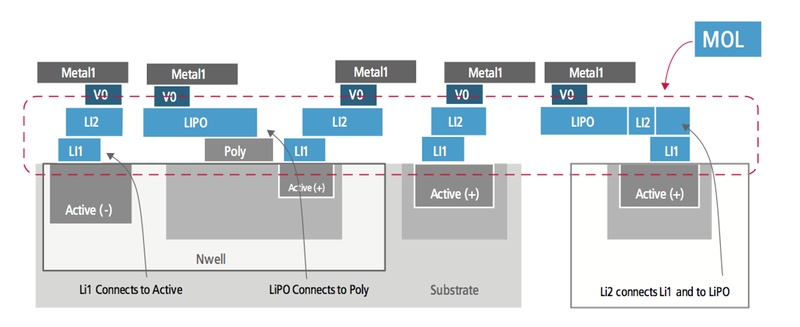
Figure 3 New types of local interconnect enable increased density at 20nm (Source: Cadence)
Designers need to be aware that MOL layers have restrictive design rules. For example, MOL shapes often have fixed directions with length constraints. The density of this interconnect also stores up issues for future nodes, such as the need to model increasingly complex parasitic effects between the device and the MOL.
Some of these issues can be overcome by careful prioritisation of which areas of a design need to be as dense as possible, and which can absorb some slack without undermining overall PPA. This prioritization enables some layers to be patterned at more relaxed dimensions, reducing the need for cost double-patterning lithography and so saving masks and hence costs.
The density of 20nm processes also exacerbates the problem of rising interconnect resistance, which demands more sophisticated layer-aware routing strategies for critical signals such as clocks.
FPGA companies Altera and Xilinx have both faced this issue in their 20nm designs, and have adjusted their logic architectures and routing strategies to overcome it.
The density of 20nm process also makes it more difficult to route to individual cells. The cell pin access problem means that designers may have to forgo some of the density gains for which they moved to 20nm, just to complete the routing.
20nm processes also demand greater use of metal and poly fill techniques to even out the impact of manufacturing techniques. Where once fill was mainly used to maintain planarity, now fill has to be used to counter the impact of the absolute density and rate of density change of both poly and metal across multiple layers. These can have undesirable effects on stress, etch rates, rapid thermal annealing (RTA) and other parameters.
Fill is also being used to manage proper light emissivity during lithography, and to regulate etch processes. The fact that more fill is being used means more polygons to be represented in database and analysed by the tools.
Doing fill on a critical layer under double patterning constraints further multiplies the number of polygons that have to be generated, represented and analysed.
This increases GDSII file sizes, and makes optical proximity correction for the fill shapes on the masks more challenging.
Each fill shape also has a capacitance of its own, and in relation to other shapes, which means more analysis and more complex fill rules to try to meet foundry density requirements while not degrading timing.
Fill requirements represent a further challenge for analog and mixed-sgnal designers, whose circuits are particularly sensitive to neighbouring polygons. Design flows have been developed for 20nm AMS design and trial chips run, and some vendors have enhanced fill tools so that they are smarter, and give users much greater control about what they do.
AMS and custom designers face a number of specific issues at 20nm and below:
Coventor’s analysis of the potential impact of double patterning on process variability (mentioned earlier) is only part of the variability story. An analysis by simulation company GSS of whether 20nm process developers should create the gate of the transistors first or last also pointed out that:
“variability results in approximately one order of magnitude increase in the average leakage current of a single transistor or in the overall leakage current of the chip compared to ideal ‘uniform’ transistors without variability”
A subsequent posting by GSS, derived from a paper by GSS founder Asen Asenov in IEEE Transactions on Electron Devices, reiterated the point, arguing that statistical variability “has killed bulk CMOS”. Sources of variability used in the analysis include the distribution of random discrete dopants, line-edge roughness, and the granularity of metal gates.
The shift from 28nm to 20nm has brought with designs that are two to four times more complex than those undertaken at 28nm, with a greater number of combinations of process parameters (corners), and a wider variety of usage scenarios – as well as the complexity brought by new manufacturing issues, as detailed above.
This demands greater accuracy in parasitic extraction,as well as more powerful static-timing analysis tools. Some vendors are suggesting a shift to a more hierarchical timing analysis approach, as a way of dividing and conquering the issue created by this growing complexity.
Test strategies are also evolving for 20nm processes to help meet the yield management challenges imposed by the node, including the increased variability of transistor sizes and threshold voltages, and interconnect resistance.
The challenges of 20nm have a number of implications: