May 21, 2019
How Mentor develops and works with partners to prepare each version of its Calibre DFM platform to be ready for the introduction of each new process node.
December 31, 2018
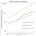
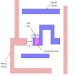
A detailed dive into how MBH strategies for litho hotspots have been enhanced to deal with double patterning at 20nm and below.
February 1, 2018
A new technique has been developed to catch potential new lithography issues when little design data is available for incoming nodes.
November 24, 2017
John Ferguson reviews the key capital metrics you need to review when deciding whether to move to a new process.
September 14, 2017
An alphabet soup of AI, HPC, 5G and the IoT has finally seeded creation of a design infrastructure for silicon photonics.
March 22, 2017
The equipment giant's Computational Process Control strategy takes a pragmatic approach to Industry 4.0 and is likely to influence EDA tools for incoming nodes.
November 29, 2016
FinFET processes and libraries are maturing, enabling designers to explore the best ways to take advantage of the capabilities of the new transistor design
October 29, 2015
The 10nm process will see changes to multiple patterning that demands changes in the implementation flow, along with an increased focus on the effects of variability.
July 20, 2015
In sessions at the 2015 Design Automation Conference, engineers who had worked on finFET-oriented projects revealed how the technology has changed their design practices and where others may want to think twice about making the move.
October 6, 2014
ARM and TSMC used an extensive pre-planning process, including a static analysis of each module's overall logic structure, to put together a 2.3GHz processor design based around ARM's main 64bit Big.Little pairing for the foundry's 16nm finFET process.