Lithography challenges threaten the cost benefits of IC scaling
Will we be able to engineer another technology node that brings the usual cost and area savings without EUV lithography? I have serious doubts.
EUV lithography was supposed to be ready for the 45nm process node, and was then delayed until 32nm and later, 22nm. Today, major semiconductor companies are continuing to develop their offerings. Some will use the upcoming IEDM to detail their 1xnm processes, developed despite the lack of EUV’s patterning capabilities.
Why the delay with EUV? The story has been told many times: a combination of complex electro-optics, problems with the power of the illumination source, resist sensitivity and defectivity. The list of EUV challenges is long, but the summary is short: it’s not ready yet!
So, we embark on another round of process development, into the 10nm node, with the same lithography systems we’ve been using since 45nm: 193nm immersion, capable of numerical apertures around 1.35. The lithographers have pulled many tricks, known as resolution enhancement techniques (RETs), out of their bags. New types of masks, new polarizations of the source illuminators, the most complex model-based optical proximity corrections on the mask patterns have all been essential to maintain 2D scaling with 193nm light. But the physics of that 193nm system fundamentally limits the 1D pitch of single exposure printing to roughly 72nm. With 10nm technologies pushing pitches down towards the 50s, meeting the challenge will take much more than just another set of RET innovations.
Two “double-patterning” techniques are emerging to tackle the patterning issue, particularly for Back End of Line (BEOL) integration, where fundamental pitches are often tighter than at the Front End of Line (FEOL), and high aspect ratios and damascene integration pose additional process challenges. This paper outlines how each of these techniques works, their potential advantages and limitations. But despite the energy and ingenuity that has gone into developing these responses to the lack of EUV, the costs associated and the yield and reliability risks from process variation will prevent many companies from achieving the typical economic advantages of scaling.
Trench-first metal hard-mask integration
Well before double patterning became necessary, there was a change in the way that BEOL integration was achieved. Up to this point, the via level (Vx) was patterned before the ‘line above’ or ‘trench’ level (Mx): Vx was etched partially, and completed during the subsequent Mx etch.
This approach had problems. The Mx lithography was done after the wafer had been patterned by Vx, creating an uneven topography requiring planarizing layers to enable further patterning. Removing the materials that planarized the partially patterned vias became increasingly damaging to the lower-K dielectrics that were being introduced at the time, reducing overall process yield and reliability.
Meanwhile, the FEOL engineers were introducing high-quality thin metallic films to enable high-K/metal-gate transistors. The BEOL engineers caught wind of this, and made a beautiful transition to a trench-first metal hard-mask scheme, in which the Mx is patterned first, but only into a thin metal hardmask. The Vx level can then be patterned last, avoiding the process of filling and stripping. The pattern is completed when the line is transferred from the metal hardmask into the dielectric. 1
This approach also enabled the partial etch of Vx to be self-aligned to the Mx hardmask pattern (creating self-aligned vias, or SAV). This reduced the extent to which Vx extended outside Mx, which was becoming a reliability issue. Semiconductor manufacturers implemented this change at various different nodes, based on patterning and reliability challenges.
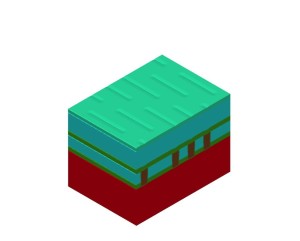
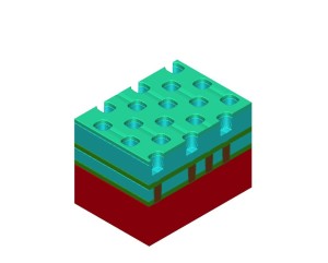
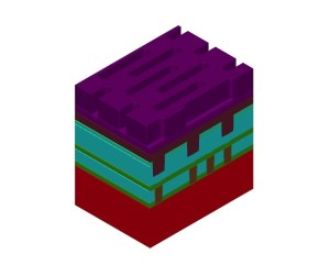
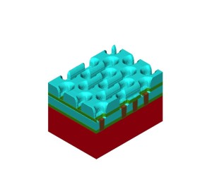
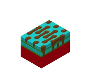
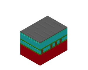
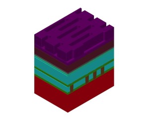
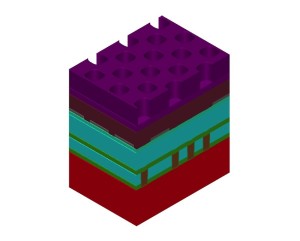
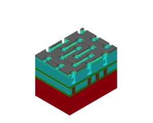
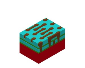
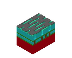
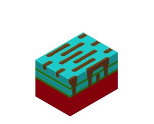
In figures 1 – 3, we use the Coventor SEMulator3D Virtual Fabrication Platform to demonstrate via-first, trench-first metal hardmask and self-aligned via integration schemes, all using single patterning.
Figure 1 – Via-first BEOL flow
-
1 – ILD films
-
2 – Via lithography
-
3 – Via partial etch
-
4 – trench lithography (note planarizing film in partially etched vias)
-
5 – trench etch (note profile ‘blow-out’ from via lateral etch)
-
6 – metal fill and CMP (note via to line proximity)
- 1 – ILD films
- 2 – Via lithography
- 3 – Via partial etch
- 4 – trench lithography (note planarizing film in partially etched vias)
- 5 – trench etch (note profile ‘blow-out’ from via lateral etch)
- 6 – metal fill and CMP (note via to line proximity)
Figure 2 – Trench-first BEOL flow
-
1 – ILD films (notice metal hardmask film)
-
2 – trench lithography
-
3 – hardmask etch
-
4 – Via lithography
-
5 – Via partial etch
-
6 – trench etch (note, no material ever deposited in vias)
-
7 – metal fill and CMP (note via to line proximity)
- 1 – ILD films (notice metal hardmask film)
- 2 – trench lithography
- 3 – hardmask etch
- 4 – Via lithography
- 5 – Via partial etch
- 6 – trench etch (note, no material ever deposited in vias)
- 7 – metal fill and CMP (note via to line proximity)
Figure 3 – SAV trench-first BEOL flow
-
1 – ILD films (notice metal hardmask film)
-
2 – trench lithography
-
3 – hard mask etch
-
4 – Via lithography
-
5 – SAV partial etch (note via shape constrained by metal hardmask pattern)
-
6 – trench etch
-
7 – Metal fill and CMP (notice improved via to line proximity)
- 1 – ILD films (notice metal hardmask film)
- 2 – trench lithography
- 3 – hard mask etch
- 4 – Via lithography
- 5 – SAV partial etch (note via shape constrained by metal hardmask pattern)
- 6 – trench etch
- 7 – Metal fill and CMP (notice improved via to line proximity)
This elegant solution to the current problems also helped simplify the introduction of two techniques developed to extend 193nm lithography to yet another process generation. Both rely on what have become known as double-patterning techniques.
Litho-etch litho-etch (LELE) double patterning
First, basic double patterning was developed. This is about as brute-force as it gets. Split the features at the densest pitch up onto two masks, pattern one, then pattern the other. This scheme is typically known as ‘litho-etch litho-etch’ (LELE) or, due to the pitch-based decomposition, ‘pitch splitting’.
With the thin metal hardmask in place, this LELE scheme simply adds steps to the hardmask etch part of the process flow. This is a relatively straight-forward approach, and has several strengths, but puts extreme pressure on the precision with which one masks aligns with the next. LELE can be used to pattern the lines and vias in a dual-damascene integrated BEOL, using a combined MxVx module. This used to require two masks, but now requires four.2
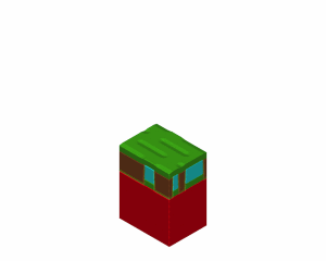
In figure 4, we use the Coventor SEMulator3D Virtual Fabrication Platform to demonstrate the process flow of an example 48nm pitch LELE MxVx module.
Figure 4 Process flow of an example 48nm pitch LELE MxVx module - click to animate (Source: Coventor)
As minimum pitches continue to be reduced, and 2D designs complicate the process of splitting these shapes up onto different masks (decomposition), LELE can (and probably will) be extended to triple-patterning and possibly even quadruple-patterning. The decomposition challenge will continue to plague the design community and drive the patterning integration.
The main challenge with LELE is lithographic alignment, and this problem strikes LELE in a few different ways. First, ‘at-level misalignment’ is a whole new problem. When lines at a dense pitch are patterned on a single mask, the process variations that impact the space between those lines are primarily lithographic dimensional bias, and etch variations. When this module is moved to LELE double patterning, those variations double (two exposures, two etches) and a new variation appears: the misalignment between the two exposures. Lithographic tool vendors continue to improve stage control and alignment procedures, but it’s impossible to completely remove this variation below 3-6nm. So, just when the fundamental line/space configurations begin to challenge reliability mechanisms, we’re adding an additional variation mechanism to the mix!
In figures 5 – 7, we use the Expeditor batch execution and Virtual Metrology capabilities of the Coventor SEMulator3D Virtual Fabrication Platform to study the reliability impacts of process variation on our demonstration 48nm-pitch LELE MxVx module.
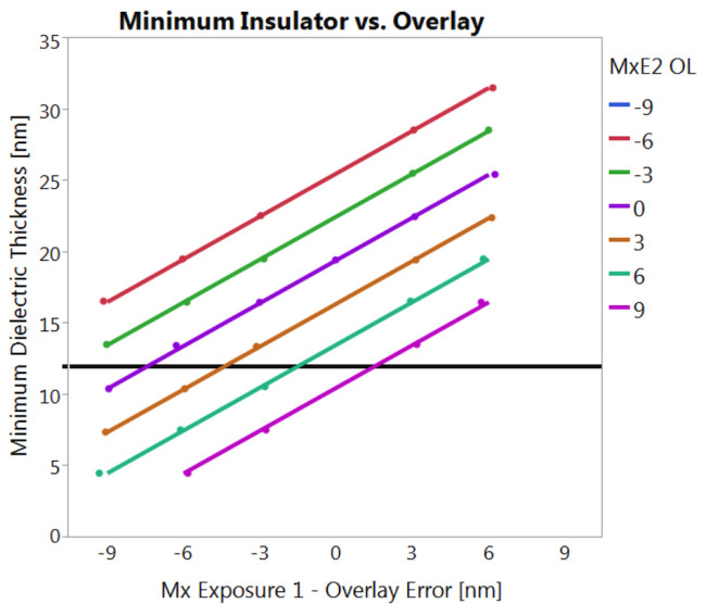
Figure 5 This chart shows the minimum dielectric thickness between Mx lines, and the sensitivity to the overlay error of the two Mx exposures. The horizontal line is at 12nm, which would support 1.2V maximum voltage at a 1.0 MV/cm breakdown field. This data shows failure when both exposures mis-register a bit more than 3nm, or if one exposure mis-registers by ~9nm, even if all other processes are perfect.
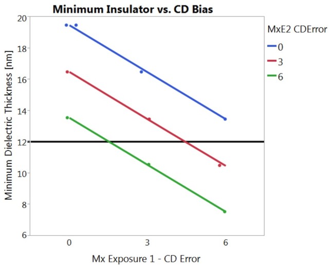
Figure 6 This chart shows the minimum dielectric thickness between Mx lines, and the sensitivity to the CD error of the two Mx exposures. The horizontal line is at 12nm, which would support 1.2V maximum voltage at a 1.0 MV/cm breakdown field. This data shows failure when both exposures are oversized by a bit more than 3nm, or if one exposure mis-registers by ~9nm, even if all other processes are perfect.
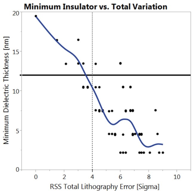
Figure 7 This chart shows the minimum dielectric thickness between Mx lines, and the sensitivity to the total lithography error of the two Mx exposures, assuming overlay is controlled at +/-2nm (1sigma) and CD is controlled at +/-1nm (1sigma). The horizontal line is at 12nm, which would support 1.2V maximum voltage at a 1.0 MV/cm breakdown field. This data shows less than 4 sigma statistical coverage to this criteria.
This misalignment problem gets worse after the first level. To what do you align the next levels? Do you choose to align both next-levels to one of the previous levels? Or, do you align one of the subsequent levels to EACH of the previous level’s exposures? This rats’ nest grows pretty complex for design and decomposition techniques. The overlay errors compound, giving subsequent levels even less process margin, further reducing yield and degrading reliability.
This LELE scheme is workable, given the lack of an EUV single-patterning option, but presents dramatic challenges to process control. The added cost of the additional patterning steps suppresses the economic advantage of technology scaling. The process variation sensitivity impacts yield, delaying the revenue stream of high-yield volume manufacturing. And, the reliability sensitivity will require additional long-term stress evaluations, further degrading the financial motivation for technology scaling.
Self-aligned double patterning (SADP)
The introduction of finFET technology and the desire for dense fin packing drove FEOL technology to develop spacer patterning or sidewall image technology (SIT), which uses a single mask with a pitch above the lithographic limit to pattern features below the lithographic limit by ‘frequency doubling’.
In this approach, a ‘mandrel’ is patterned at twice the desired metal pitch. Then spacer deposition and etch processes are performed on that mandrel, similar to a historical gate/spacer process flow. But in the spacer patterning flow, the mandrel is then removed, leaving only the spacers to mask subsequent etches. Because each mandrel shape gives rise to two self-aligned spacers, the subsequent etches deliver patterns at the desired pitch (half the pitch of the mandrel patterning).
For one-dimensional features (i.e. lines), this flow seems pretty straightforward, but once two-dimensional designs are considered, the challenge becomes clear. Each mandrel shape results in a loop of freestanding spacer. It’s nearly impossible to completely pattern the wide range of available BEOL design constructs with this as the hardmask. So, an additional level of lithography is required to ‘block’ additional areas, and create real BEOL patterns. This additional block-level lithography is performed after the spacer definition, but before the final hard-mask etch. 3
This approach alleviates the problems of multi-exposure and associated overlay misalignment, but comes with its own issues. And in the BEOL, in a damascene (subtractive) process, with its complex and flexible set of designs, even spacer patterning requires an additional exposure. This scheme is typically referred to as ‘self-aligned double patterning’ (SADP), because the features are self-aligned due to spacer patterning, but a second exposure is still required to form all the required design constructs.
While this scheme can be used to pattern the line levels, it’s not clear that there’s a way to use it to pattern vias. So, even a well-developed SADP Mx integration typically requires a LELE Vx integration.
In figure 8, we use Coventor SEMulator3D Virtual Fabrication Platform to demonstrate the process flow of an example 48nm pitch SADP Mx module, using a LELE Vx integration.
Figure 8 Process flow of an example 48nm pitch SADP Mx module, using LELE Vx integration - click to animate (Source: Coventor)
In SADP, the overlay issue inherent to LELE integration is eliminated. Adjacent lines are self-aligned to one another through spacer patterning. However, this is a much more complex patterning technique. Now, rather than just the standard lithography and etch variations, there are far more sensitive processes involved. The spacer deposition thickness and sidewall conformality become critical patterning parameters, as does the uniformity of the spacer etch. These additional new variations contribute both to increase the width of the metal lines (to achieve resistance, opens yield, electromigration goals) and to increase the thickness of the dielectric between them (to overcome capacitance, shorts yield, TDDB concerns).
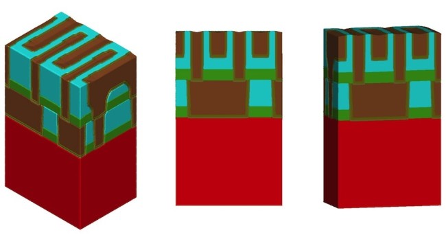
Figure 9 SEMulator3D Model of 48nm-pitch SADP BEOL with 10% thin spacer deposition, 10% sidewall coverage deficit and slightly aggressive lateral etch. The isometric view (at left) shows how adjacent lines behave differently due to spacer variations (grow/shrink). The cross-sectional view (centre) shows a risky 11.5nm insulator spacing at the top of adjacent line. The slight-tilt view (at rght) is included for completeness.
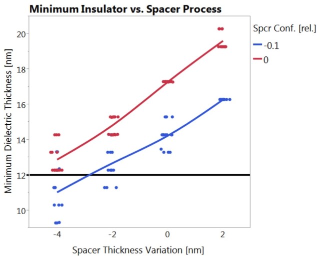
Figure 10 This chart shows the minimum dielectric thickness between Mx lines, and the sensitivity to the spacer deposition thickness and con formality. The horizontal line is at 12nm, which would support 1.2V maximum voltage at a 1.0 MV/cm breakdown field. This data shows failure when the spacer is ~3nm too thin and 10% less conformal than target, even if all other processes are perfect.
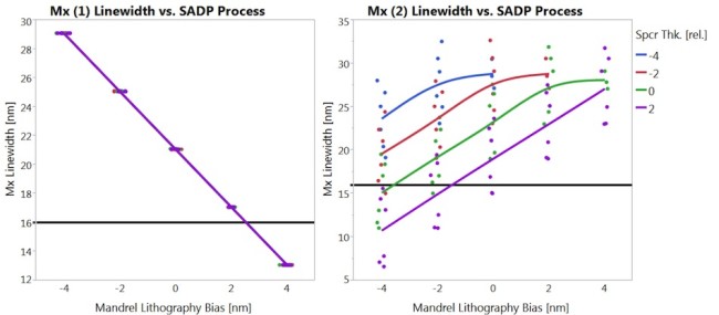
Figure 11 This chart shows the linewidth of two adjacent Mx lines, and their sensitivity to SADP processes. Since one line is patterned by the mandrel, its linewidth is dictated by the lithography process. The adjacent line is subject to many more process parameters, giving adjacent lines very different sensitivities to the same process variations. The horizontal line at 16nm represents a hypothetical electrical limit with resistance ~20% above nominal.
LELE design decomposition sounds pretty straightforward, but can become challenging once real 2D constructs are considered. SADP decomposition, on the other hand, is difficult to think about, even for simple designs! The SADP ‘spacer plus block’ integration scheme does not intuitively lend itself to mask decomposition, so complex algorithms are required. And, since the BEOL requires a wide array of design constructs to facilitate local and global routing, these algorithms will be tested to the limit. (see fig 1 from Zhang, et. al., DAC 2011)
Again, it’s pretty clear that SADP can work, and that an amazing amount of engineering talent will be required to make it successful. That said, the complexity of this scheme will increase the cost of the resulting technology, due to increased process cost, narrow yield margins and long development cycles.
Conclusion
Advanced technologies are getting much more difficult and even the most experienced process developers are having very public setbacks. Amazing innovations are emerging to breathe further life into Moore’s law scaling, but the question remains whether the economic benefits of scaling will be realised. Advanced modeling capabilities, such as Coventor’s SEMulator3D Virtual Fabrication Platform used here, will be essential to speeding technology development cycles and avoiding costly and time-consuming learning cycles in the fab. Without these advantages, development expense could wipe out the narrow financial margins on these technologies
Double patterning (and eventually the triple- and quadruple-patterning schemes that will become necessary if EUV continues to be delayed) will lead to higher process costs, narrower yield margins, greater reliability risks, longer development times and complex design processing algorithms. These complexities will increase wafer cost and reduce the die-area scaling of advanced technologies. These are the key components of the economy of scaling, and without EUV, they’re just not adding up!
All the examples in this article are based upon public information available in the references in the text.
Author
Dr David M Fried is Chief Technology Officer – Semiconductor at Coventor, responsible for the company’s strategic direction and implementation of its SEMulator3D Virtual Fabrication Platform. His expertise touches upon such areas as silicon-on-insulator (SOI), FinFETs, memory scaling, strained silicon, and process variability. Fried holds 45 patents and spent 14 years at IBM, most recently as 22nm Chief Technologist for IBM’s Systems and Technology Group. He has Bachelors, Masters and Doctoral degrees in electrical engineering from Cornell University.
Company
1000 Centregreen Way – Suite 200Cary, NC, 27513
Phone: (919) 854-7500 x 132
Fax: (919) 854-7501
 Dr David M Fried is Chief Technology Officer - Semiconductor at Coventor, responsible for the company’s strategic direction and implementation of its SEMulator3D Virtual Fabrication Platform.