Power and clocking at 20nm force changes in FPGAs
Design for the 20nm generation of processes has revealed power and clocking issues for the two major FPGA manufacturers presentations at Hot Chips revealed. Xilinx decided to use additional metal layers to overcome the growing problem of interconnect resistance. Altera implemented programmable back bias control into its Arria 10 FPGAs to try to save power and used time-borrowing flip-flops to deal with clock skew on long wires.
Steve Young, lead architect for FPGA fabrics at Xilinx, said: “We are going through an inflexion point as we shrink. Metal resistance is becoming an issue. But we need the metal to speed up along with the transistors.”
To avoid RC delays slowing down logic blocks connected by relatively long wires, Young explained by adding more metal layers to the design, “it has allowed us to implement more routing tiles with longer wires. By using more metal layers we are able to use more of the thicker traces to reduce resistance, rather that having a few finer-pitched layers. This is becoming increasingly important as we move into new generations”.
Brad Vest, director of IC engineering at Altera, said the designers undertook strategic planning to ensure that critical signals got the lowest RC paths through the power mesh. He added that the designers moved back to tristatable signals for long lines to help maintain performance in the presence of RC increases. Previous generations of FPGA had moved away from the tristatable lines.
Distributed clocks
Although some designers have expressed concern over the power demands of the following generation based on finFETs and whether this would necessitate further changes in the metal stack, Young told Tech Design Forum the better performance of the core transistor meant that it should be possible to reduce active power consumption for a given logic structure.
Young explained how the company rearchitected its clocking structure and configurable logic blocks to help deal with interconnect issues in its 20nm-generation FPGAs. “Every few generations we grow the logic blocks and within the blocks themselves we have made several innovations. For example, we have doubled the number of clock-enable signals as clock gating has become more prevalent in designs.”
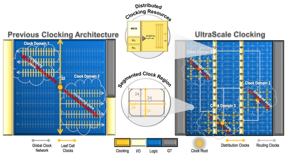
Image Changes to the clocking architecture for Xilinx' 20nm FPGAs
The use of more complex configurable logic blocks (CLBs) is moving hand-in-hand with the evolution of tools that favor the use of a small number of dense blocks connected at a local level. This, said Young, reduces average wire lengths and provides greater flexibility for the blocks that need to interface with long-distance traces.
For the latest parts, Xilinx has moved to a distributed clocking approach to reduce the effects of clock skew encountered with the use of a small number of global clocks.
Vest said for Altera’s 20nm-generation parts, the company “need some clock flexibility to provide place and route [tools] with greater flexibility”. Part of the change in the logic structure involved moving from a tile-based structure to one built around columns of either hardened logic blocks or CLBs. Time-borrowing flip-flops have helped deal with the skew on long metal traces, Vest said.
More logic complexity
Like Xilinx, Altera has found it profitable to make the CLBs more complex. “The ratio of logic to flip-flops varies dramatically among customers,” Vest said, but the company has been tracking growth in the use of flops overall. “Last generation we put in more registers and that decision has been borne out. We have now doubled the number of flip-flops that we have in our fabric.”
To deal with power consumption, Altera opted for body bias techniques. Tools analyze the logic for critical paths and bias the transistors for paths that do not need such strict timing “so they don’t burn as much power”, Vest said. “The granularity of bias control is down to every pair of logic blocks.”
To deliver the bias voltages to each CLB pair, the on-chip power network delivers several voltage levels with power muxes employed to drive each local block to the right value.
Vest said the use of double patterning and associated restrictive design rules called for changes in approach to place and route: “I know that it was very painful for our engineers. We had to put in a lot of methodology and a lot of systematic techniques to overcome the double patterning problem. We had to take significant advantage of structured-custom layout. It is more streamlined than a standard custom layout.”
Vest added: “We also had to face a lot more variation so we did more statistical analysis of the design.”
Variation concerns led Altera to put more resources into digitally assisted analog techniques. “Previously we use soft microcontrollers [implemented in the FPGA fabric] to drive calibration. Now we have added two hard microcontrollers to do that, which also enables calibration before the FPGA is programmed,” Vest said.