14nm FD-SOI pushes strain and body bias for power savings
At the VLSI Technology Symposium in Honolulu CEA-Leti, IBM and STMicroelectronics described the 14nm version of the FD-SOI they have developed as the follow-on to the 28nm process currently being prepped for production at GlobalFoundries and Samsung Semiconductor, as well as ST’s Crolles, France fab. The process provides better support for body-bias techniques and incorporates germanium for a faster PMOS device.
The companies claim the 14nm process provides 0.55x area scaling compared to the 28nm node, effectively using the same process and layout infrastructure as the 20nm process developed by the Common Platform partners and shown in their 2012 VLSI Symposium paper. That process added features such as local-interconnect layers – now standard on 20nm-class processes – and constructs that allowed tighter placement of common standard-cell features. The contacted poly pitch is 90nm, with double patterning used for a 64nm-pitch metal-one layer.
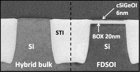
Key changes from the 28nm process are strain and mobility enhancements to increase drive current, particularly for p-channel FETs, as well as the decision to bring bulk areas of the wafer – where the oxide of the original wafer sandwich is removed – up to the same level as the SOI active layer.
Image Cross-section of 14nm FD-SOI process showing planarized bulk and SOI sections
On the original 28nm process, the oxide was etched away, providing access to a bulk silicon substrate at a slightly lower level. By bringing the bulk layer up through epitaxy, the team claims the 14nm process odes not “induce surface penalties”. The hybrid layer can be used to implement body biasing, now seen as key to the competitiveness of FD-SOI, as well as ESD-protection devices and various passive devices.
Strained SOI
Papers presented at the 2012 VLSI Symposium showed that strain could be viable for FD-SOI, including one technique that was not expected to work so well: silicon germanium in the PMOS channel. The 14nm FD-SOI has incorporated silicon germanium into the p-channel devices while the n-channel devices remain silicon. A germanium-enhanced nFET is on the cards for the 10nm process according to recent presentations.
At IEDM, the STMicroelectronics, CEA-Leti, IBM and GlobalFoundries team reported a current drive of 670µA/µm for p-channel devices at 0.9V against an Ioff of 100nA/µm. At a lower voltage of 0.8V, the Ion level in the full process has fallen to 405µm/µm but with a lower leakage of 20nA/µm, when demonstrated in a ring-oscillator circuit. Gate length tuning from 20nm to 34nm provides leakage control over three decades.
On the basis that gate-drain capacitance is major contributor to speed, particularly in ring oscillators, the process uses a raised source-drain structure as well as process tweaks to control poly thickness. The result is a process that is about 20 per cent faster than the 28nm version but with a 100mV lower supply.
The process designers expect power savings and speed to go further thanks to the combination of body bias techniques and the option to select from two threshold voltage settings for the transistor. The well designs are designed to match reverse body bias (RBB) with LVT devices, to minimise leakage and forward body bias with SLVT for performance. The bias voltage in the preferred direction can be pushed to the breakdown voltage of the NP diode in the well – amounting to about 5V.
According to the team, devices running with a supply of 0.6V with a 2V FBB are as fast as those operating at 0.8V without no bias. For the same dynamic power consumption, a 14nm circuit can provide a frequency boost of 30 per cent, or for the same frequency cut dynamic power by 55 per cent. Reducing the supply voltage by a further 150mV and applying 2V FBB provided a further dynamic power cut of 40 per cent in one experiment.
