Cell pin access
Since the introduction of the 40/45nm generation of processes, the design rules that control the lower metal layers have become increasingly complex and context-dependent. Although many of these rules may be considered optional by foundries, they generally need to be followed to ensure high yield as insufficient clearance between metal lines and vias can lead to shorts, for example.
Double patterning adds an additional set of restrictions as not only yield factors but coloring rules may make certain combinations of shapes in the local-routing or metal layers impossible to achieve. As a result, layout approaches for connecting lower metal levels to the pins that worked in previous generations may no longer work. This has a knock-on effect on the design and use of standard cells as previously good designs can become very difficult to work with.
Design rule constraints mean that even a cell designed for good pin access may not be easily routable if surrounded by other cells that restrict access. At ARM TechCon 2013, Paddy Mamtora, product engineering group director at Cadence Design Systems, said: “The same cell that should be a good cell but which is used in a bad neighborhood can cause its own problems.”
Paul Cunningham, Cadence R&D vice president, described the problem at TSMC’s OIP in October 2013, recorded by Brian Fuller of Cadence in a blog on Cunningham’s presentation: “It’s getting harder and harder to cut them close together. You get a larger and larger halo around each via cut before we can cut a neighboring via. If we’re trying to turn a corner on the same layer, to escape from a via then we have to have a certain minimum distance. We can’t turn a sharp corner.”
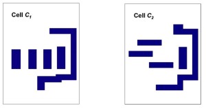
Figure 1 Examples of notionally 'good' cells at 45nm (Source: IBM Research)
IBM researchers described the problem in 2010 arising on 45nm-class processes, noting that pins that sit along a line parallel to the preferred direction of metal above can be almost impossible to connect, even for that generation, because routing needs to be used on upper layers to connect to all of the pins. A cell of this type is shown as C1 in Figure 1 above. A staggered layout of pins oriented 90° to the metal direction should be easier to route, depicted by the example of C2 above. However, conventional quality metrics such as pin density that attempt to analyze the routability of cells based on the ratio of pins to cell size will rarely pick up on the problem.
Global versus local routing assessment
A further problem is that the routability assessment of a design has traditionally been dominated by global routing concerns. Global routing prediction tends to use tile-based algorithms that do not analyze routing that stays within each tile. In effect, local routing congestion is invisible until the detail router is called into action at which point multiple rip-up and retry runs may be needed.
In a DAC 2012 paper, Li et al from IBM Research described the problem: “When a high number of signal pins are fully contained within a global routing tile, it is a good candidate area for potential local pin access problem. One interesting observation is that the pin density map [can be] quite discrete compared to the global routing congestion map. In the global routing congestion map, the level of congestion [may change] gradually while in the pin density map, one hot congested tile sits right next to a cold one with no congestion at all.”
Pin access can be improved by increasing the spacing between cells, at the cost of increased area and cost, by changing cell locations so that they are split across global routing tiles to allow sufficient routing capacity to be allocated to each one but with a potential cost in terms of increased wire delay, or by redesigning the cells themselves to offer greater accessibility. It is currently unclear as to whether tools may have to take into account multiple versions of a standard cell that offer better pin accessibility depending on their surrounding environment.
Taraneh Taghavi from IBM Research developed a cost function described at ICCAD 2010 that is better suited to assessing local routing congestion caused by pin-access problems. Tools are adopting congestion metrics based on pin accessiblity to guide cell selection and placement ahead of detailed routing.
