Preparing for success at the next node with Calibre
How Mentor develops and works with partners to prepare each version of its Calibre DFM platform to be ready for the introduction of each new process node.
The push toward every new semiconductor process node requires all participants to follow a path of continual improvement, innovation, and preparation.
Foundries must focus on characterizing new devices, implementing new process tools, and developing new process flows. They must work with EDA companies to ensure that qualified design enablement tools and decks will be available.
Design companies must focus on defining circuit functionality and setting performance and reliability targets. They work with EDA companies to ensure there are new ready-to-use versions of the verification software and hardware needed to enable design signoff in reasonable turnaround times and profitable yield after manufacturing.
All these changes place ever-increasing pressure on EDA companies to provide foundry-qualified tools that expand automated verification functionality while maintaining the highest level of accuracy – and that do this without driving up runtimes.
Let’s take a closer look at the challenges of next node development for EDA companies. We’ll examine how Mentor, a Siemens Business, prepares the Calibre nmPlatform for each new node.
Challenge One: Set the bar
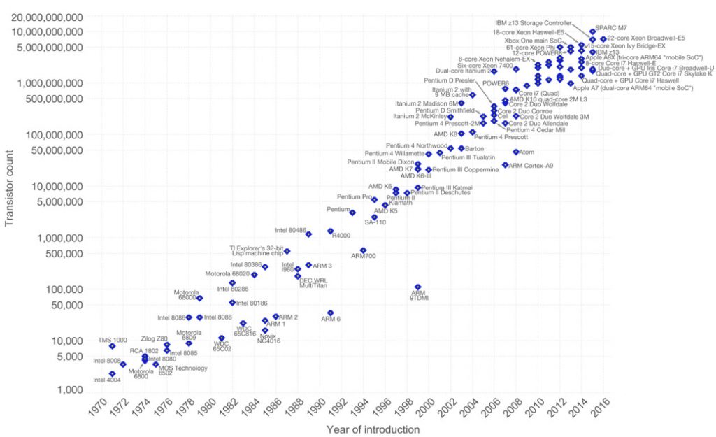
Pretty much since its inception, the semiconductor industry has used transistor count as a measure of its progress. Moore’s Law arose from the observation that transistor count in an IC design approximately doubles every two years. Figure 1, a composite graph of the transistor count of the most well-known IC chips over time, shows that Moore’s Law growth continues, with the most modern chips now nearing counts of 20 billion transistors [1].
Another measure, overall polygon count, is actually more important to EDA companies because the complexity of design rule checking (DRC) is directly proportional to the number of polygons in a design. While transistor count has a direct impact on the number of polygons in layers at the front-end-of-line, it does not account for the increase in the overall polygon count of today’s designs. The middle-of-line (MOL) and back-end-of-line (BEOL) layers also have more polygons per layer, and advanced process nodes also have more interconnect layers – and therefore more polygons. Verification tools must contend with polygon counts that are growing much faster than transistor counts.
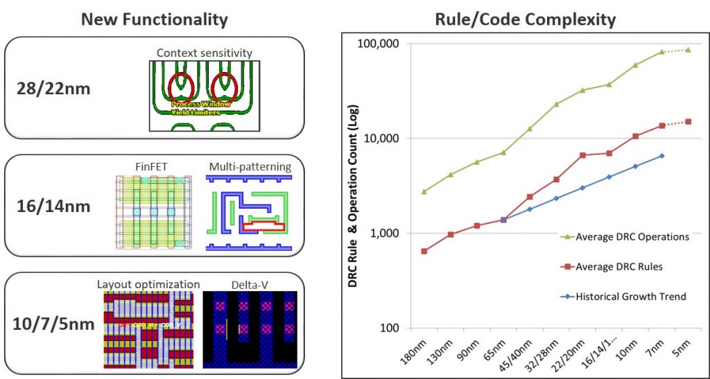
The total number of design layers or polygons is not the only factor in verification. The types of verification issues applicable to any given layer have also increased over time, as more complex, context-aware, and variation-sensitive design components and process techniques have been introduced. Figure 2 shows a few of these techniques and design sensitivities that require not just more checks, but entirely new types of checks. When we pair the increase in layer count with the increase in the types of checks, we can see how both the number of design rules and the operations needed to implement those rules increase from process node to process node. Because each check requires many lines of code to implement, the ‘average DRC operations’ line on the chart shows the number of steps the software has to execute to properly apply those checks to a design.
We know that the computational power and resources needed to verify a modern IC are driven by the total polygon count of the design multiplied by the number of design rules and their complexity, so we can begin planning to deal with this challenge. This is the time to examine each element, and think beyond previous solutions to find innovative opportunities to expand and improve the overall performance and productivity of the verification toolset. EDA companies must continually add fundamental new capabilities into their tool base to provide accurate automated checking of these expanded requirements, while still enabling design companies to meet market deadlines.
Challenge Two: Build the base
In EDA, the two most obvious components needed to overcome the compute challenge are raw engine speed and memory. For example, the Calibre nmPlatform tool suite has been around for decades in name, but the underlying code base is continually optimized, and has even been completely rewritten. This is not just to add or enhance functionality, but also to dramatically improve the performance of existing functionality and take advantage of modern distributed and cloud-computing infrastructures.
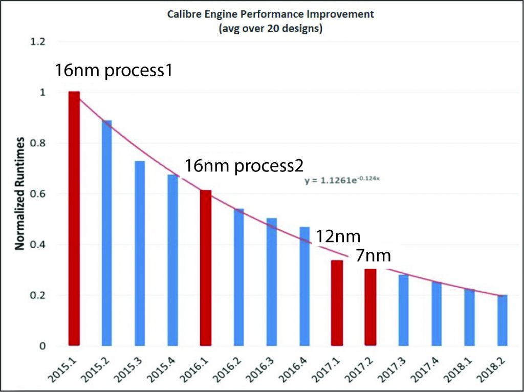
If we consider engine speed as the first component of base performance, we can look at that metric over time to evaluate relative improvement. Figure 3 shows a trend of normalized runtimes for the same Calibre nmDRC runset by software version release. Each data point consists of an average of 20 real-world customer designs, demonstrating (by holding everything else constant) the isolated improvement of the underlying Calibre engine over multiple releases. Over this three-year time span, engine speed increased by 80%.
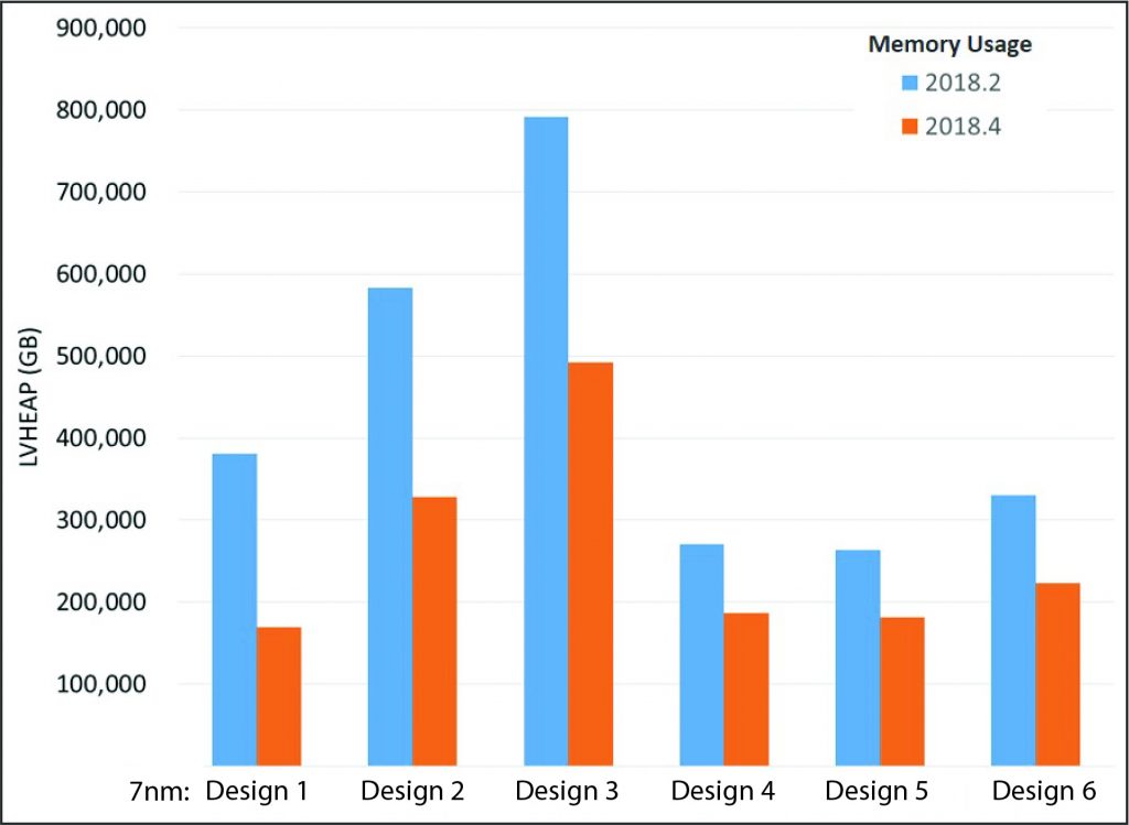
Memory usage is the next key aspect of improving performance. Figure 4 compares two recent Calibre nmDRC versions across six different 7nm designs. There has been a consistent 40-50% decrease in memory usage between versions as underlying data structures and memory management techniques have been improved. Even though the Calibre nmPlatform is the industry leader in memory efficiency, maintaining leadership requires constant effort.
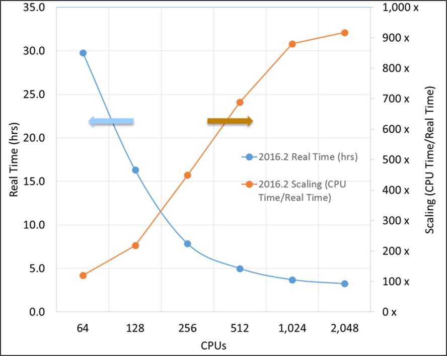
Once an EDA company has done all it can to improve the base engine performance, it must confront the explosive growth in computational requirements. Effective utilization of modern compute environments and distributed CPU resources helps increase overall compute power. Figure 5 demonstrates the gains achieved by constantly pushing the Calibre platform’s capability to effectively scale over larger and larger numbers of CPUs. The graph represents a full-chip Calibre nmDRC run for a production customer’s 16nm design based on the appropriate foundry rule deck.
The Calibre platform maintains its industry-leading performance through the combination of continuous runtime, memory, and scaling performance improvements in the underlying engine. And yet, even this is not enough to keep up with the rising complexity of the most advanced process nodes. Now the team must bring their expertise and experience to bear and search out less obvious opportunities for improvement.
Challenge Three: Collaborate with partners
Foundries
The choice of tool that foundries use to develop their processes and the supporting design rule decks and semiconductor intellectual property (IP) matters.
Why? The analysis and development of new checking capabilities takes time. Maturing new functionality and processes into a verification flow with high performance, low memory, and superior scaling takes longer. An EDA company with customers working on the leading edge cannot wait until the next node is entirely ready before it integrates the required capabilities into its verification tools, or those customers will miss the early market. Conversely, it cannot successfully develop robust new functionality based solely on an early snapshot of a developing process. Foundries learn as they go during process development, a process that frequently changes the requirements for verification tools.
So, one of the critical components for any EDA vendor as it prepares for the next node is to be in lockstep with the foundry as it creates that node. The most valuable return from a foundry partnership for Mentor is to have the foundry use Calibre tools as they develop a new process node. That real-time, iterative cycle of trying the new functionality, then evaluating the results with Calibre tools helps the foundry fine-tune the design requirements, and enables the Calibre team to update their verification tools, long before design customers begin using them.
This collaborative learning benefits customers. For example, the foundry’s ‘golden’ DRC tool is used to develop and verify IP through early versions of the sign-off deck. The foundry uses the DRC tool to define and validate the new process design rules, validate all IP developed by the foundry, and develop and validate the regression test suite with which other DRC tools will be validated. The thousands of DRC runs and tens of thousands of checking operations involved help hone the accuracy of the foundry’s ‘golden’ DRC tool and helps set the standard for other DRC tools seeking qualification for that node. This typically happens months to years before those other DRC tools can even begin their validation. Think of it this way—if the Calibre nmDRC tool was an athlete, both it and its associated foundry deck would have 10,000 hours of experience and training before any other DRC tools even got to the track.
If a design house uses different verification software from that the foundry used during process development, it will have to wait until after the process node is nearly production-ready for the tool vendor to have learnt about and implemented the required changes in its tool. That, in turn, means their customers’ designs will lag the commercial introduction of that process node. Certification is on one of the opportunities that comes from being a foundry’s training partner.
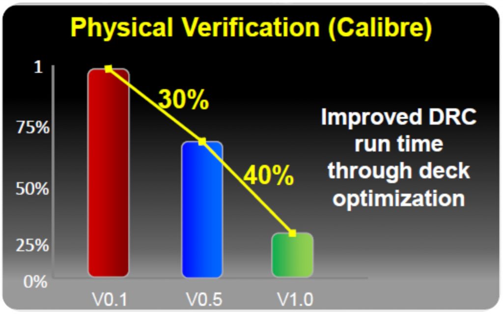
One way of measuring this advantage is to look at the performance of DRC decks across the pre-production release cycle. Physical verification tools are, at their core, a specialized programming language for writing DRCs. Working with the foundry teams that write the design rule decks and the foundry engineers that use those decks as the decks are being written enables the Calibre team to identify opportunities for coding optimizations. The resulting foundry decks are already well-optimized when the process goes into production. Figure 6 shows just how much deck optimization can affect runtime for the Calibre nmDRC tool. Version 1.0 (the first full production version) of the deck runs nearly 70% faster than version 0.1. This improvement is the result of coding optimizations identified during deck development.
Foundry partnerships enable Mentor to offer IC design companies Calibre tools and decks that provide the best possible performance and highest accuracy achievable.
Design Companies
It can be easy for an EDA company to fixate on the basic function of checking in isolation, because that is what performance and accuracy metrics primarily focus upon. However, measuring performance in isolation does not capture the impact on the tool in use, and the overall turnaround-time (TAT) required to reach a clean tape-out. TAT is often the metric that matters most to design companies.
One way to respond to the increased complexity of each new node is to increase the productivity of IC designers. Most design companies have teams located around the world, using various implementation tools. The design industry knows that each EDA company has a few strong tools, and others that have yet to be optimized for leading-edge designs. So they use the best tool for each verification task in the design flow, rather than relying on a single vendor.
To make this strategy work well for designers, the tools must prioritize functional, seamless integration over proprietary formats and interfaces. In physical verification, for example, integration should include the ability to configure, launch, review, and debug within the design tool environment, regardless of which design tool is used. It is important, for example, that tools which handle operations such as multi-patterning coloring (which includes back-annotation of assigned colors) and fill (in which fill data is generated in the native format of the design tool), can both stream-out results and offer batch execution. The verification tool must also run inside the design tool, directly on the design database, as if it were a native part of the design tool integrated directly onto the toolbar.
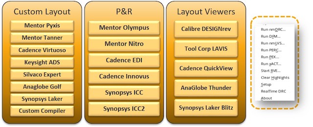
Verification tools such as the Calibre nmPlatform are built to be independent of the design tool, so computer-aided design teams can integrate them easily into best-in-class tool flows. They can use Calibre interface tools to piece together entire flows that facilitate and automate fill, multi-patterning coloring, chip integration, and engineering change orders, just to name a few. Figure 7 shows the broad range of Calibre nmPlatform integration with other EDA design and implementation tools.
Designers also need easy-to-use tools. Usability is more than just making it easy to launch jobs and get results. Isolating fundamental issues in early-stage designs can be overwhelming. Trying to find errors in chip integration when the IP blocks are still buggy is frustrating. Debugging errors revealed by checks on multi-patterning, delta-voltage, and antenna issues is extremely difficult. Even managing, navigating, and visualizing all the complex errors that occur in leading-edge design nodes is critical. New features such as special debug layers for double-patterning debugging, or automated waiver processing for masking out IP errors during chip integration, can save designers hours of debug time and frustration, and often reduce time-to-market more than improving raw tool performance.
Conclusion
Meeting the challenge of preparing for the next process node takes expertise in the traditional skills of software performance, memory and scaling, and skills in partnering with foundries and designers to optimize tools and flows for overall productivity and performance. By combining continuous software improvement and innovation with foundry and design-company partnerships, Mentor is always prepared to overcome the ongoing challenge of the next node.
Further Reading
IC Design: Preparing for the next node
References
[1] Max Roser and Hannah Ritchie (2019) – “Technological Progress”. Published online at OurWorldInData.org. https://ourworldindata.org/technological-progress
About the authors
Michael White is the director of product marketing for Calibre physical verification products at Mentor, a Siemens business. Prior to joining Mentor, he held various product marketing, strategic marketing, and program management roles for Applied Materials, Etec Systems, and the Lockheed Skunk Works. Michael received a B.S. in System Engineering from Harvey Mudd College, and an M.S. in Engineering Management from the University of Southern California.
David Abercrombie is the marketing director for multi-patterning applications at Mentor, a Siemens business. Prior to joining Mentor, David managed yield enhancement programs in semiconductor manufacturing at LSI Logic, Motorola, Harris, and General Electric. David received a BSEE from Clemson University, and an MSEE from North Carolina State University
