October 27, 2017
How to address increasingly complex patterning issues and debug them efficiently as design moves toward 12 and 10nm.
October 3, 2016
Multi-patterning, finFETs and more are forcing more detailed overhauls of P&R software at each process node. We dig into some of the key new issues and how they are being addressed.
October 29, 2015
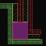
The 10nm process will see changes to multiple patterning that demands changes in the implementation flow, along with an increased focus on the effects of variability.
July 20, 2015
In sessions at the 2015 Design Automation Conference, engineers who had worked on finFET-oriented projects revealed how the technology has changed their design practices and where others may want to think twice about making the move.
August 12, 2014
Sign-off lithography verification is vital as we move beyond double to multi-patterning but changing responsibilities in the flow must be handed with care.
January 20, 2014
It is not just a choice between EUV and multiple patterning for future nodes, but even between varieties of multi-mask technologies. How will you decide?
January 13, 2014
If EUV is further delayed until 8nm, the industry has to explore other options for patterning, and the effects they will have on the DFM flow.
December 3, 2013
The costs of advanced lithography techniques at 1xnm, and the yield and reliability risks from the resultant process variation, will stop many companies getting the typical economic advantages of scaling.
August 25, 2013
What ARM learnt when it ran a Mali GPU-based test chip through a Synopsys tool flow onto a TSMC 20nm process
April 22, 2013
The arrival of the 20nm and finFET-based 14nm and 16nm processes bring with them challenges for custom IC design. These are the five key areas and a methodology that can address them.