IEDM keynote: cost scaling will swap architectural changes for area
The keynote given by ARM senior principal research engineer Greg Yeric at IEDM 2015 highlighted the cost issues that face the semiconductor industry and the growing reality that future scaling relies on the ability to harness heterogeneous technologies in parallel.
Although the first 50 years of Moore’s Law “were, in retrospect, rather straightforward”, according to Yeric, the next ten still present opportunities for integration that can more or less follow the historical trend.
Yeric claimed the CMOS part of the industry is likely to follow a cost trend that lies between the two extremes of cost scaling stopping completely at 28nm and Moore’s Law continuing along a straight line. Instead, for 10 million unit volume and above, the cost per transistor will fall but more slowly.
At the 10 million volume level, the average drop may be just 10 per cent per generation from 28nm to 7nm. This is not good news for constant die-area scaling. Even at very high volume – 300 million or more – cost for a 1cm2 die could rise more than 20 per cent per node from 28nm down to 7nm. This is assuming that EUV will be delayed until after the introduction of 7nm but that the cost of multiple patterning will be less than today by the 7nm node because of throughput improvements and greater efficiencies in mask preparation.
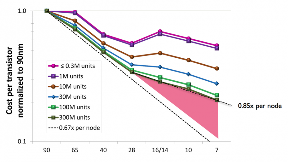
Image Cost per transistor reduction scenario to 7nm (Source: ARM)
The trends are not helped by problems further scaling SRAM. Even if the bit cell can be made physically smaller in principle, variation and parasitics make it difficult to reap the full benefits of the remaining area scaling. Increases in wire resistance will demand more metal layers as well as a reduction in the maximum length of the wires, making memory arrays less efficient.
Yeric argued that the increased cost of metal routing may encourage greater investment in MOL routing layers to improve routing flexibility around the transistors. He suggested that logic process developers might even borrow the buried wordline concept from DRAM. Design-technology co-optimization would provide a way of using the available structures more efficiently.
A further problem is energy consumption, which will result in an increasing proportion of the silicon having to remain ‘dark’ at any time. Because transistor scaling will not reduce power consumption much from now on, architectural changes will be needed to deliver the required energy savings.
Changes in memory technology towards high-density, low-energy non-volatile memory and compute architectures that are more tightly coupled to memory – either by embedding processors inside memory arrays or close connections through 3DIC technologies may, Yeric argued, point a way to further integration without relying on pure transistor scaling. It would be, to a large extent, a return to Moore’s IEDM 1975 prediction that “design cleverness” would provide a significant proportion of technology scaling.