January 20, 2014
It is not just a choice between EUV and multiple patterning for future nodes, but even between varieties of multi-mask technologies. How will you decide?
January 13, 2014
A number of effects have led to a dramatic increase in interconnect resistance in the sub-32nm process nodes that demands the use of smarter routing.
January 13, 2014
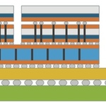
Increasingly complex design rules in 14nm and 16nm make it harder to connect local routing to the inputs and outputs (pins) of standard cells.
January 13, 2014
If EUV is further delayed until 8nm, the industry has to explore other options for patterning, and the effects they will have on the DFM flow.
December 9, 2013
Extracting finFET parasitics means a shift to 3D models, field solvers for greater accuracy, and MCMM techniques.
December 3, 2013
The costs of advanced lithography techniques at 1xnm, and the yield and reliability risks from the resultant process variation, will stop many companies getting the typical economic advantages of scaling.
October 11, 2013
PGA has been IC-centric for mainstream 2D configurations. It must become system-centric for 2.5D and 3D systems.
October 8, 2013
Electrically aware layout tools provide a more efficient alternative to time-consuming rip-up-and-retry practices in mixed-signal nanometer IC design.
October 2, 2013
New layout-dependent effects (LDEs) arise at each process node. This methodology updates LDE parameters and uses on-the-fly simulation for early detection.
May 8, 2013
Many design teams are looking at ways in which they can make use of 3D integration. Here are eight requirements for an effective 3D-IC design flow.