Eight requirements for 3D-IC design
Many design teams are looking at ways in which they can make use of 3D integration. Here are eight requirements for an effective 3D-IC design flow.
3D-ICs promise “more than Moore” integration by packing a great deal of functionality into small form factors, while improving performance and reducing costs. It’s no surprise then that many design teams are looking at ways in which they can make use of 3D integration.
3D-IC packages may accommodate multiple heterogeneous die, such as logic, memory, analog, RF, and micro-electrical mechanical systems (MEMS). Each of these die can use different process nodes, such as 28nm for high-speed logic and 130nm for analog. This provides an alternative to system-on-chip (SoC) integration, potentially postponing an expensive move to a new process node for all of the functionality developers want to place in a single package.
While there is great interest in this emerging technology, development is still at an early stage. There are clear requirements that an effective 3D-IC flow must satisfy to bring the cost, integration and performance benefits that the technology promises.
Use of the TSV, for example, introduces design, integration and test challenges. TSVs are copper vias with diameters that may range from 1 to 30um, and they make it possible to integrate multiple stacked dies in a single package.
With 3D-IC, a die containing TSVs can be attached to the package substrate using conventional flip-chip technology. A second die is attached to the first using the TSVs to route connections — not just to the adjacent IC but to the underlying PCB through the package’s redistribution layer.
Compared to a wire-bonded system-in-package (SiP), 3D-ICs constructed using TSVs offer reduced RLC parasitics, better performance, more power savings, and a denser implementation. Compared to a 2.5D silicon interposer approach, a vertical 3D die stack offers a higher level of integration, smaller form factor, and faster design cycle. But a 3D stack raises some additional challenges, including thermal, timing, and power management concerns.
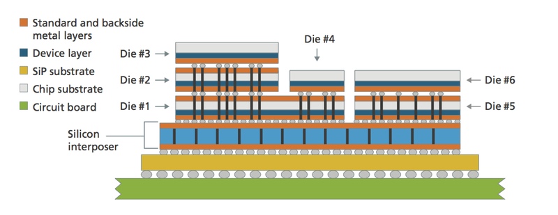
Figure 1 3D integration can support complex stacking arrangements
Although 3D-ICs with TSVs do not require a revolutionary new 3D design system, they do require some new capabilities that need to be added to existing toolsets for digital design, analog/custom design, and IC/package co-design. The end goal is to optimize system cost with the shortest possible turnaround time. If 3D-ICs cannot be both cost and time effective, they will not enjoy widespread adoption. To that end, we have identified and are working toward supporting eight requirements for design tool flows that support 3D-IC:
1. System-level exploration
The cost and benefits of 3D-IC can be subtle as there are many tradeoffs that engineering teams can use during design to bring some functions onto a monolithic die that will make economic sense under certain circumstances. In other cases, the desire for flexibility or to reduce design risk can favor the migration of functions to other die within a single package.
Sometimes called ‘pathfinding’, 3D-IC system-level exploration will help users partition designs into separate chips, select the appropriate silicon technology for each chip, determine where functionality goes, choose the best die order in the stack, and optimize connectivity between chips.
Existing system-level exploration tools can provide early power, area, and cost estimates, and allow what-if explorations across architectures, silicon IP choices, and foundry processes. These tools are being to serve stacked die implementations and package considerations and to carry this intent through the design process.
2. 3D floorplanning
Once the technology selection and partitioning choices have been, floorplanning is vital. Although the pin-to-pin distances within a package are much shorter than those of PCB traces, the decisions over type of integration and how functions are distributed will have direct impacts on performance.
For example, TSVs are very large compared to logic gates and other circuit features. Thus, the number and location of TSVs is crucial. With too many TSVs, the wire length goes up. TSVs cause coupling, which can be reduced by adding space to their keep-out zones – but this adds to the area. TSVs also cause mechanical stress, which can impact the performance of nearby devices.
Given these considerations, a TSV-aware 3D floorplanning capability is quite challenging. It must provide an abstraction level to capture all the die, and provide a unified representation of intent for placement and routing tools.
A 3D floorplanner should work in the X, Y, and Z directions, and should have visibility into the top and bottom of each die. This helps optimize the placement of blocks, TSVs, and micro-bumps, and shortens interconnect distances, thus improving performance and power. For continuous design convergence, micro-bump and TSV assignments should take into account the floorplans on adjacent die.
Ideally, a 3D floorplan will be aware of thermal issues and will help avoid hotspots. It will also help users determine the optimal placement of die into stacks. The order of the stack is important. Die in the middle are most susceptible to thermal problems.
3. Implementation
The techniques used by tools for synthesis, placement, and routing change in the 3D-IC environment. For example, there are new layout rules that may be driven by features on adjacent die. The back-side redistribution layer (RDL) is a new layout layer. And given their size, TSVs themselves are a significant new layout feature.
A digital implementation system that supports 3D-ICs must be “double-sided aware,” taking into account both the top and bottom of each die. This may call for a new modeling and database infrastructure, TSV-specific tools, and support for a variety of stacking styles.
Power planning for a single-die IC is hard enough. With a 3D stack, it gets more complex. Designers need to provide enough power to drive all of the die, including the top-most die. Designers must manage vertical voltage drop and reliably simulate system power consumption. Tools need to support power distribution for TSVs and micro-bumps. A unified representation of power intent should be carried across the entire 3D-IC design.
Place and route tools should include thermal constraints to avoid hot spots. Routing tools need to handle TSVs and micro-bumps properly, route signals across multiple die, and verify the bump alignment between adjacent die.
Managing clocks across multiple die while avoiding skew is another challenge. If there are different clocks for different die, the designer must figure out how to synchronize them.
Analog implementation environments also need to add support for 3D-ICs. Examples of useful capabilities include multi-chip visualization with background views; support for bump, TSV, and reverse-side routing; and connectivity extraction maintained through TSV connections.
Throughout the design convergence process, design intent must be maintained and checked, and the necessary abstraction techniques must be applied for proper implementation and analysis.
4. Extraction and analysis
Extraction and analysis tools are crucial for design convergence in any IC-design environment. However, existing extraction and analysis tools need to be extended for 3D-ICs. For example, the tools must consider RLC parasitics for TSVs, micro-bumps, and interposer routing. Further, analysis tools must be 3D-aware. Timing, signal integrity, power, and thermal gradients must be analyzed across multiple die. Multi-die static timing must be validated, with an understanding of interactions between multiple die and with the package.
Because the metal stack creates heat gradients, thermal analysis and signoff is critical, especially for die located in the middle of the stack. Further, the substrate thinning required for 3D stacks results in relatively poor heat dissipation. After placement and routing, thermal signoff is needed to ensure hot spots are below specified limits, and that thermal effects do not have a negative impact on performance or leakage.
Signoff raises new questions with 3D-IC stacks. For example, can design rule checking (DRC) and layout-versus-schematics (LVS) run on the entire stack? Can timing be verified for the entire stack? Is there any crosstalk between die?
Electromagnetic interference (EMI) is a possible concern for 3D-ICs, raising a potential need for analysis tools. A multi-die package offers less shielding than a single-die package, and thus offers more likelihood that emissions could escape.
Finally, to facilitate TSV connections, the wafer is thinned to implement a 3D-IC. This causes stress and adds susceptibility to thermal changes, which need to be accounted for in the design.
5. Design for test (DFT)
Test raises many challenges for 3D-ICs, including access to die inside a stack and proper handling of thinned wafers. Both new standards and tool support are required to help validate that design intent is maintained once 3D-IC silicon is realized, and to diagnose issues properly if the system doesn’t behave as intended.
Like conventional single-die IC test, 3D-IC test must be considered at two levels – wafer test (for the silicon die), and package test (after die assembly into the package). The difference is that in the 3D-IC fabrication, there are many more intermediate steps, such as die stacking and TSV bonding. This provides many more opportunities for wafer test before final assembly and packaging.
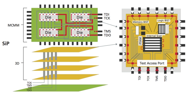
Figure 2 Test access for a 3D stack requires pre-planning
Wafer test is needed for cost optimization. If a die is bad, it can be thrown away before it is placed in a package. If a package-level test fails, the entire package would have to be thrown away. Thus, wafer test is highly desirable, especially early in the product lifecycle while defects may still be relatively high.
But wafer test for 3D-ICs is challenging for three reasons. First, today’s probe technology is unable to handle the finer pitch and dimensions of TSV tips, and is generally limited to handling several hundred probes, whereas the TSVs may have several thousand probes. Second, probe technology leaves scrub marks that can potentially cause problems with the downstream bonding step. Finally, wafer test requires the creation of a known-good die (KGD) stack. To stack known-good die, the wafer must be thinned by about 75 per cent so the tips of the TSVs can be exposed. However, as the thinned wafer is contacted by a wafer probe, there’s a danger of damaging the wafer.
3D-ICs also introduce new intra-die defects. These may be introduced by new manufacturing steps such as wafer thinning, or by bonding the top of a TSV to another wafer. Thermal effects are another potential sources of defects, because excessive heat may be generated from the densely packed stack of dies. Thermo-mechanical stress is caused by different thermal coefficients of the various materials in the stack. Despite the differences in the manufacturing steps, the resulting faults (shorts, opens, delay defects) appear to be similar to what we see in conventional ICs. It is possible that new fault models may be required as we get more empirical data.
Modeling defects through TSV-based interconnects is a new area. These defects may be introduced in the fabrication or the bonding of TSVs. Fortunately, defects introduced through TSVs can be mapped to existing fault models, such as opens, shorts, static, delay, and bridging faults. However, a methodology is needed to map TSV defects to known fault types.
A sound methodology for 3D-IC test includes a DFT architecture that provides efficient ways to control and observe individual die from the chip I/Os, while providing different test access modes (such as a mode for a known good die test or a known good stack test). Conventional DFT architectural approaches and techniques such as on-chip compression, boundary scan, memory built-in self-test (MBIST), reduced pin count testing, and on-chip clocking for at-speed test are broadly applicable, and need to be configured and optimized to meet 3D controllability and observability goals. The trick is one of making an intelligent allocation of DFT resources across the multiple die to minimize the area overhead, while meeting constraints for test cost and shipped product quality.
6. IC/package co-design
Developers of 3D-ICs need to remember that any electronic product includes three different fabrics – chips, packages, and boards. Designing the chip first and throwing it “over the wall” to package and board designers will not result in design convergence on an optimal, cost-effective solution.
If the chip, package and board are not designed co-operatively, the interconnect will not be optimized, and extra vias will be needed to handle signals that cross from one point to another. As a result, performance will be reduced, additional board layers may be needed, and board and package costs may rise. Further, without co-design, timing, power, and signal integrity will not be optimized.
IC/package co-design is important for 3D-ICs because there are a large number of I/Os, and because the cost of packaging goes higher with multiple die in one package. Without co-optimization, the package could end up costing more than the silicon die. Important capabilities include I/O feasibility planning, connectivity management, 3D visualization, SiP layout, and support for multi-fabric analog and RF circuitry. To ensure complete design convergence, the packaging tool must understand the IC and package design intent, and should effectively abstract the IC design database to provide constraint-driven layout of the package substrate.
The board must be considered as well. 3D die stacks result in additional interconnect that will have to find its way down to the board. As more connectivity is handled inside the package, there’s less complexity on the board. The board designer needs to know what’s going to be positioned near the 3D package. By positioning and rotating components properly, the designer can reduce the number of layers required for the board.
Some companies drive co-design from the board up. They know where components will go on the board, and those locations are fixed. They then design the package that contains the stacked die in order to optimize connectivity, and to allow the minimum number of layers on the PCB. But it’s not so important where co-design starts – what’s important is that it is done to assure convergence for the 3D-IC silicon-realization process.
7. A flexible ecosystem
To be successful, 3D-ICs need to be designed and produced in a cost-effective way, with sufficient turnaround time to meet market windows. This will be possible only with a robust and well-defined supply chain ecosystem, including semiconductor design companies, EDA vendors, IP suppliers, foundries, and outsourced semiconductor assembly and test (OSAT) providers.
Boundaries between the different players may start to blur. For example, when are TSVs created and who is responsible? Possible implementation steps include:
- Via first – wafer processing starts with TSVs and is done by the foundry.
- Via middle – TSVs are created after transistors, but before back end of line (BEOL), by the foundry.
- Via last – TSVs are created after BEOL, probably by the OSAT.
Since one size does not fit all with 3D-ICs, the supply chain needs to be adaptable to customer needs.
Many customers will want to line up a second-source 3D packaging service provider before production is started. Additionally, key strategic alliances between memory suppliers, logic IDMs, foundries, and packaging subcontractors will need to be forged.
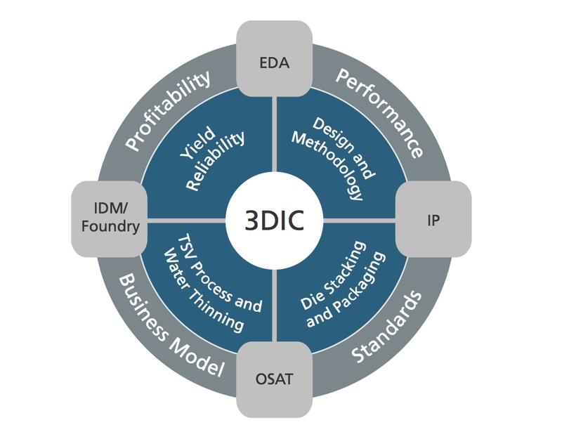
Figure 3 Effective 3D-IC design requires collaboration
Foundries are establishing design rules, create models and libraries, and provide process design kits (PDKs) and reference flows. One example of a design rule is to avoid placing TSVs too close to active devices, because they cause mechanical stress that may change the performance of the device. Tools must be aware of recommended TSV diameters and pitches. They need to understand distances between TSVs as well as the width of metal routing to TSVs.
OSATs will play a role in assembling early 3D stacks and interposer configurations, combining die from different foundries, and developing tests for 3D stacks – but in the long term they will have to compete with foundries who are pulling OSAT tasks in-house.
8. 3D-IC standards
Standards will become an important part of the 3D-IC ecosystem. An initial standards effort may focus on defining a taxonomy of terms. Down the road, I/O standardization between interfaces such as memory, logic, and interposer layers will be helpful.
Meanwhile, the 3D-IC Alliance is focusing on the manufacturing side, and has released the Intimate Memory Interconnect Standard (IMIS) to standardize vertical interconnect requirements. Another area calling out for standardization is 3D-IC test. Two emerging standards – IEEE 1149.7 compact JTAG and IEEE P1687 internal JTAG (iJTAG)—can be deployed together to embed test structures in 3D-ICs.
The IEEE 1500 standard for embedded core test makes the pins of an IP core controllable and observable.
The same principle could potentially be used to access individual die in a 3D stack. The IEEE 1500 “core test wrapper” concept places a DFT wrapper around a core. In a 3D-IC, this concept could place an entire die in a wrapper and make it accessible through a product-level I/O interface. The same test patterns could be reused at the package test level.
Conclusion
From a design standpoint, the good news is that extensive retooling is not needed for 3D-ICs. Although there are clear requirements for 3D-IC development, the fundamental underpinning for tools is in place. There is no need to acquire a new ‘3D’ design system. There are also no apparent showstoppers in process technology. However, new capabilities are needed in the areas discussed above, such as architectural analysis, floorplanning, place and route, thermal analysis, timing, signal integrity, IC/package co-design, and test.
Above all, a comprehensive solution is needed. Many 3D stacks will combine digital and analog/RF circuitry, requiring a strong analog/mixed-signal capability. Because of the unique packaging requirements of stacked die, an IC/package co-design capability is a must. Additionally, fitting 3D-ICs on a board is challenging, requiring a capable PCB layout system with appropriate analysis tools. Thus, anyone who presents a complete “solution” must provide expertise in digital, analog, IC, package, and PCB design.
About the author
Steve Carlson is marketing group director for silicon realization at Cadence Design Systems.
Contact
Cadence Design Systems
2655 Seely Avenue
San Jose, CA 95134
T: +1 (408) 943 1234
W: www.cadence.com
