April 22, 2013
The arrival of the 20nm and finFET-based 14nm and 16nm processes bring with them challenges for custom IC design. These are the five key areas and a methodology that can address them.
April 10, 2013
It’s time to take up the challenge of applying 3D integration technology to IC design. The manufacturing process technology is maturing, the tool chains are in place, and the opportunities to broaden your market by applying a new form of systemic integration are growing.
April 1, 2013
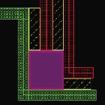
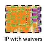
You can waive some physical verification errors related to legacy IP found in foundry DRC checks. Knowing which has involved lengthy manual analysis. TSMC is enhancing the process with automation.
December 4, 2012
finFETs are vital to the next generation of CMOS processes from Intel, TSMC and others. How will process issues including bulk vs SOI substrates, density limitations, thickness control, and planar device integration affect their practical implementation?
December 3, 2012
CSR used a customized approach to automated dummy fill layout for AMS to address layer density and device matching issues in standard flows aimed at digital SoCs.
October 11, 2012
Manufacturability, routing, library design and more - it all needs rethinking at 20nm, writes Tong Gao of Synopsys.
October 9, 2012
Finding and fixing double patterning problems in 20nm designs
September 12, 2012
A look at the way in which key tools, in IC implementation, modeling and extraction, and physical verification, are developing in response to the challenges of 20nm design
September 6, 2012
Antun Domic of Synopsys tackles the three key challenges of 20nm processes: design complexity; the physics of lithography; and economics.
August 21, 2012
A guide to emerging 3D integration techniques for ICs, including a look at various approaches, and some of the tools and standards issues involved.