Catching layout-dependent effects on-the-fly
New layout-dependent effects (LDEs) arise at each process node. This methodology updates LDE parameters and uses on-the-fly simulation for early detection.
The scaling available with the latest process nodes provides unparalleled integration and the ability to support gigahertz-frequency analog electronics – but designers have found it increasingly difficult to unlock this performance because of the rise of various types of layout-dependent effect (LDE) since the introduction of the 65nm process technology. In previous technology nodes, the main and maybe the only reasons for deviation of the post-layout simulation results from the requirements were routing parasitics. LDE-related problems now play a major role in analog and mixed-signal design, putting much more of the focus on the physical placement of devices with respect to one another.
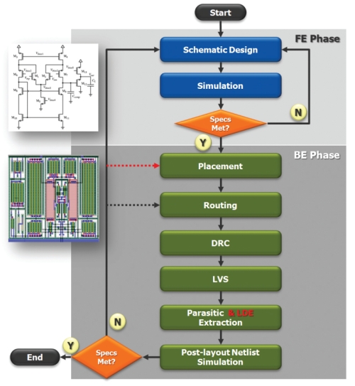
Because of the nature of LDEs, current custom-IC design flows (Figure 1) do not detect their impacts until very close to the end of the design cycle — when the schematic has been translated to a near-complete layout. Because LDEs can cause dramatic shifts in properties such as threshold voltage, significant changes will need to be made to the schematic to overcome these proximity effects. Resolving mismatches between post-layout simulation and the requirements may call for new placements for parts of the design and, of course, rerouting has to follow. This process can take a number of iterations. Accordingly, the time-to-market for many design products has increased.
Therefore, a new methodology is required to shorten the design cycle and provide early awareness for schematic designers about how LDE will impact their design. This methodology allows the early detection of LDEs during schematic creation by providing a link between the front-end phase and the back-end phase of the design flow. It accurately calculates LDEs by interfacing interactively with an analog mixed-signal simulator.
This flow was tested on a 40nm operational transconductance amplifier (OTA) design. This test case established that not only is this approach as accurate as post-layout analysis, but also equal to or better in speed of execution. Moreover, it demonstrates the practicality of using on-the-fly simulation to detect and resolve LDEs early in the design flow.
Figure 1 The typical custom IC design flow
On-the-fly simulation
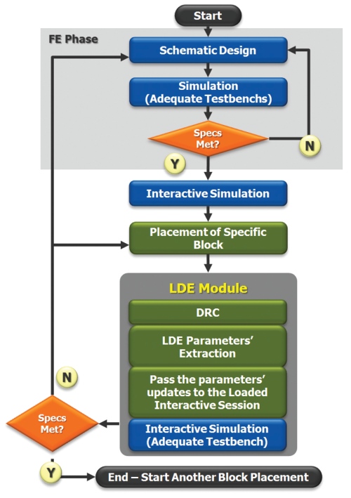
On-the-fly simulation makes slight modifications to the current custom IC design flow in order to reduce the design cycle. This solution involves running an analog and mixed-signal circuit simulator, such as Eldo from Mentor Graphics, in interactive mode in order to reduce simulation time by eliminating system process launching time.
Figure 2 On-the-fly simulation for the detection of layout-dependent effects
The operation begins by creating the schematic and the required testbenches needed to verify the functionality of the design. Then an interactive simulation session begins. The circuit nodes, models, and specified testbenches are loaded and stored in the memory space of the simulator. Once in place there is no need to incur the overhead of re-loading this data if only the parameters of the devices change. Schematic designers can try different device placements and can examine the impact of any specific configuration of device placement on the original specifications by opening a layout session using Eldo’s LDE module. The LDE module is responsible for a number of activities. It will extract a device’s layout-dependent parameters based on their configuration in the layout, automatically feed these changes to the simulator’s interactive session to reflect the impact of LDEs as the design changes, and compare the results to the reference results from the front-end simulation.
If the results after re-running the simulation are unacceptable, the designer can easily change the layout configuration or the original schematic device parameters to meet the original design specifications. After that, the schematic designer can set constraints for the placement of the device for the subsequent steps in the design flow.
Efficiency and performance
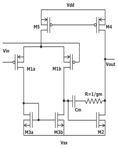
To prove the efficiency of the proposed technique, we undertook two experiments. The first experiment set out to demonstrate the impact of the layout-dependent effects on fulfilling the design requirement specifications. In this experiment, we used a simple two-stage OTA design (Figure 3) implemented using the 40nm technology.
Figure 3 Schematic design of two-stage Miller OTA (biasing network not shown)
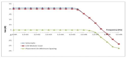
As shown in figure 4, the original DC gain of the design, when the LDE effects were ignored, was about 47 dB. After adding the effect of the LDE parameters on a placement optimized for minimum spacing, the DC gain of the amplifier dropped to around 5 dB. There are two reasons behind this degradation: the first was ignoring the LDE effects during the schematic design, and the second was the placement of the devices with respect to each other in the layout.
Figure 4 Bode plot for the OTA design
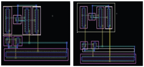
The curve with 5 dB gain was obtained after the devices were placed with the minimum allowable DRC distance between them, as indicated in the layout on the left in figure 5. Then, a number of placement combinations were tried to resolve the problem using the fast LDE module. We were able to achieve a better placement, as shown in the layout on the right in figure 5, which yielded a gain of 45 dB, as indicated in figure 4. So, finding a fast way to compute the LDE effects for different placement topologies and calculate the impact of this placement on the circuit characteristics on-the-fly is a considerable aid to the circuit designer.
Figure 5 The OTA layout placed on minimum spacing is shown on the right. The modified layout after using the LDE module is on the lef
The second experiment was conducted to prove the performance gains achieved by using the new methodology. For that, we used a moderate size 2 Kbit RAM cell, which contains around 14,000 MOS devices, running DC operating point analysis. After each placement, the LDE module updated the device parameters and launched on-the-fly simulation. This on-the-fly interactive simulation demonstrated a significant speed advantage for this application.
Conclusion
Layout-dependent effects not encountered in the design flow of previous process nodes cause design failures. A novel methodology based on updating the LDE parameters for all the devices in the design and launching on-the-fly simulation allows early detection of the layout-dependent effects and provides a clear speed advantage.
About the author
Ahmed Ramadan has worked at Mentor Graphics for 16 years. His area of focus is device modeling, reliability, simulation and parameter extraction. He has been a member in the Compact Model Coalition (Si2) for 14 years and is currently the chairman of the Compact Model Coalition’s Reliability Working Group. Ahmed earned a B.Sc. in Electronics and a M.Sc. in Device Physics from Ain Shams University in Cairo, Egypt. He holds an MBA from the American University in Cairo.
Contact
Mentor Graphics
Corporate Office
8005 SW Boeckman Rd
Wilsonville
OR 97070
USA
T: +1 800 547 3000
W: www.mentor.com
