July 26, 2012
How Cadence, Intel and Xuropa accelerated the semiconductor design process by squeezing 15% more capacity out of a virtualized server farm
July 5, 2012
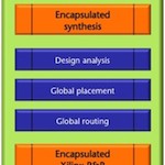
Using a new design-partitioning tool and stacked-silicon interconnect FPGA to develop an ASIC prototyping platform that can be reprogrammed several times a day.
June 1, 2012
There's still debate over certain aspects of the 20nm node, but the main challenges are already being addressed. Expect to see foundries and vendors mark their turf at DAC.
May 22, 2012
Guest blogger Jeff Wilson discusses some of the subtleties involved in the effective use of dummy fill in deep sub-micron IC designs.
May 22, 2012
Correlating production test failure diagnosis with DFM analysis can help identify and understand systematic yield issues, and to find out whether they are linked to DFM violations.
May 15, 2012
Using UML to define a software-defined modem SoC in terms of decoupled constraints - the order of activities, the timing they have to meet, and the available resources
March 28, 2012
It may be necessary to move to three-dimensional 'FinFET' transistors for future process nodes, but what impact will this have on circuit design?
March 28, 2012
Fully depleted silicon on insulator (FD-SOI) transistor architectures may offer speed and power advantages, at the cost of a shift to non-standard substrates.
January 16, 2012
Double patterning provides an alternative to using EUV lithography – making it possible to implement ICs on sub-28nm processes.
October 19, 2011
The launch of a broad-based IDM/foundry consortium that is to prepare for the shift to 450mm wafers already offers some hints as to the future shape of chip manufacturing and the planning demands it will impose on all design managers in the near future. The game is shifting from pay-for-capacity to outright pay-to-play for those [...]


