Effective finger-pointing: the art of modern yield analysis
Correlating production test failure diagnosis with DFM analysis can help identify and understand systematic yield issues, and to find out whether they are linked to DFM violations.
Since the dawn of the semiconductor industry, manufacturers have successfully ramped silicon yield at each process node, using yield-management systems (YMS) and physical failure analysis (PFA). When the majority of the industry shifted from being integrated devices manufacturers (IDMs) to fabless semiconductor companies, a new yield improvement strategy was adopted: Blame the Foundry. The logic is that all designs that meet design rule checks (DRCs) should be equally manufacturable. Poor yield is therefore the fault of the foundry.
Blaming the fab no longer works. An internet search on ‘28nm yield issues’ reveals that leading manufacturers are still overcoming the challenges involved in shipping the desired quantities of 28nm products. While it is obvious that making bigger chips with smaller transistors is complicated, one key disruption is the dramatic increase in the number and complexity of design-sensitive defects. A simple picture of a defect can no longer tell you the root cause of a yield problem. Each new design introduces additional variability (i.e. defects). Several design or process corrections may be tried before a defect is fully understood. The ability to effectively separate design- and process-oriented yield issues, and to identify the most effective corrective action, is therefore an important part of the yield-analysis process. Resolving these design-induced systematic defects is one of the few ways that fabless semiconductor companies can directly improve yield.
Enter a new DFM-aware yield-analysis flow that combines production test failure diagnosis with DFM analysis. It enables engineers to identify and understand systematic yield loss, and to determine whether the systematic yield loss is correlated to DFM violations. While the concept of combining design and silicon test analysis has been around for years [1], the problem has only recently touched a large portion of the industry and so driven the creation of practical solutions.
The DFM-aware yield-analysis flow
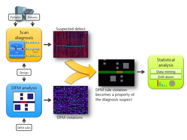
The DFM-aware yield-analysis flow is outlined in Figure 1. Test data from failed devices is used to perform diagnosis. A diagnosis tool uses the design data, production test patterns, and tester data to identify the defects causing test failures. The diagnosis tool provides information such as defect classifications and suspected defect locations[2], showing, for example, that a particular device failed manufacturing test due to an open defect in a net segment that spans metal3, via3, and metal2, and giving the coordinates of each of these polygons.
Figure 1
Overlaying scan diagnosis and DFM analysis results (Source: Mentor Graphics – click image to enlarge)
At 40nm and below, most designs are adopting some degree of DFM, and foundries are adding DFM sign-off requirements, almost as a form of risk insurance. IP and chip designers are often given a set of rule-based DFM guidelines based on a rule-deck provided by the foundry, such as GLOBALFOUNDRIES’ Manufacturing Analysis and Scoring (MAS) deck[3]. In theory, the more of these guidelines that are followed the higher the yield.
One of the features of a DFM analysis tool is to identify design features that violate these guidelines. These layout locations represent features that are expected to have greater sensitivity to manufacturing variability. When a test diagnosis result is correlated with the DFM analysis results, any DFM rule violations occurring in the same location are identified and become a property of the diagnosis suspect for that particular failing device. The diagnosis result example described above becomes “an open defect in a net segment that spans metal3, via3, and metal2 and overlaps with a violation of DFM rule m2_rec_sp”.
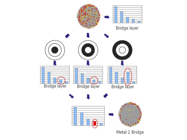
The last step in the flow is a statistical analysis that makes the volume diagnosis results actionable. One approach is zonal analysis, illustrated in Figure 2. With this approach, the individual signatures from diagnosis can be extracted and analyzed separately. For instance, out of a total population of failing devices, the tool determine how many devices were diagnosed to fail due to various defect types, such as bridges, opens, and cell defects. The tool can further separate these by metal layer. For a random defect distribution, it is to be expected that the relative distribution of a particular defect type is the same across the wafer. If the distribution of die with a specific defect, such as bridges in metal 2, is significantly different than the overall distribution of failing devices, you have a systematic defect. This type of analysis of diagnosis results is described in more detail in [4, 5]. The zonal analysis can also be used to determine whether systematic yield loss is caused by DFM violations, and to identify the most sensitive DFM rule [6].
Figure 2
Zonal analysis identifies hidden systematic yield limiters (Source: Mentor Graphics – click image to enlarge)
Enabling DFM-aware yield analysis
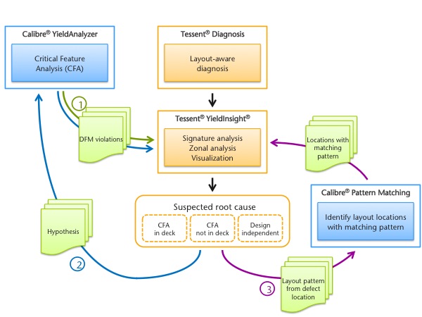
The components of Mentor Graphics’ DFM-aware yield analysis flow are shown in Figure 3. Three main categories of systematic defects can be identified with this process:
– Systematic defects that correlate with existing critical feature analysis (CFA) rules. This process will find the rules most sensitive to systematic defects.
– Systematic defects that, based on PFA or layout analysis, are suspected to be sensitive to CFA but do not correlate to existing rules.
– Design-independent systematic defects.
Figure 3
The Mentor Graphics DFM-aware yield analysis flow (Source: Mentor Graphics – click image to enlarge)
The most intuitive way to use this flow may be to correlate failing devices with an existing rule deck, as indicated in (1) in Figure 3. Although valuable, there are many cases in which the yield-limiting design feature has not already been modeled. This issue is addressed by being able to feed new rules and hypotheses back into the analysis addresses continuously. The initial analysis may, for instance, reveal a systematic issue associated with open defects in metal 3. Analysis of different die with defects in different locations may reveal that all the defects contain the same or similar design structures, which are suspected of causing the defect. Based on this hypothesis, you can create additional rules and identify violations to these rules, as indicated in (2) in Figure 3. Instead of developing new rules, you can also use pattern matching to identify other locations with the same structure [7], as indicated in (3) in Figure 3. Using either of these approaches, the original diagnosis results can be updated with the new violations, and the material re-analyzed to determine whether the yield loss correlates to the newly defined rule.
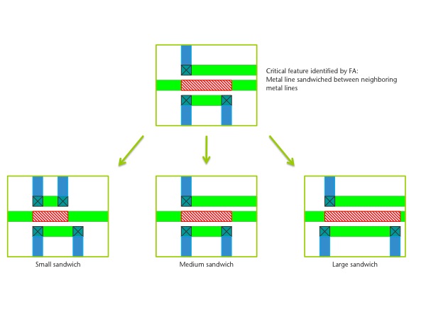
One final aspect of the flow is the ability to fine-tune rules that are shown to correlate with yield loss. The example in Figure 4 demonstrates this: if a particular design feature correlates with yield loss, you can test the data with variants of that feature to determine which version is to blame. This analysis lets you validate and refine a hypothesis without any additional PFA. An alternative approach would be to perform PFA on a very large number of devices to prove that the initial hypothesis was not a coincidence.
Figure 4
Finding the DFM feature that best describes yield loss (Source: Mentor Graphics – click image to enlarge)
Conclusion
Combining volume scan diagnosis, DFM analysis, and statistical analysis of the combined data makes for an effective yield analysis flow. The diagnosis-driven yield analysis methodology can reduce the time to root cause of yield loss by 75 – 90%, compared with traditional methods. The ability to include and continuously add DFM analysis results to the process enables the separation of design- and process-oriented yield loss.
References
[1] J. Mekkoth, M. Krishna, J. Qian, W. Hsu, C.-H. Chen, Y.S. Chen, N. Tamarapalli, W.-T. Cheng, J. Tofte, M. Keim, “Yield Learning with Layout-aware Advanced Scan Diagnosis,” Proc. of International Symposium of Testing and Failure Analysis (ISTFA) 2006, pp. 208-418. www.asminternational.org
[2] Y.-J. Chang, M.-T. Pang, M. Brennan, A. Man, M. Keim, G. Eide, B. Benware, T.-P. Tai, “Experiences with Layout-Aware Diagnosis — A Case Study,” Electronic Device Failure Analysis, May 2010, pp. 12-18.
[3] D. Payne, “Third Generation DFM Flow: GLOBALFOUNDRIES and Mentor Graphics”, August 26, http://www.semiwiki.com/forum/content/743-third-generation-dfm-flow-globalfoundries-mentor-graphics.html
[4] C. Schuermyer, B. Benware, G. Rhodes, D. Appello, V. Tancorre, O. Riewer, “Device Selection for Failure Analysis of Chain Fails Using Diagnosis Driven Yield Analysis”, Proc. of International Symposium of Testing and Failure Analysis (ISTFA) 2011, pp. 91-97. www.asminternational.org
[5] S. Palosh, G. Eide, “Scan diagnostic analysis assist SoC fab debug/process monitoring”, SolidState Technology, July 2011, pp. 22-255.
[6] C. Schuermyer, S. Malik, and T. Herrmann, “Identifying Systematic Critical Features Using Silicon Diagnosis Data”. Semi Advanced Semiconductor Manufacturing Conference, 2012. http://semi.omnibooksonline.com
[7] “Calibre Pattern Matching: Picture it, match it…done!”, Mentor Graphics Whitepaper. www.mentor.com
About the Author
Geir Eide earned a BS and MS in electrical and computer engineering from the University of California at Santa Barbara and is a product marketing manager in the Silicon Test Solutions group at Mentor Graphics.
About the company
Mentor Graphics Corporation8005 SW Boeckman Rd.
Wilsonville
OR 97070 USA Ph.: 503-685-7943
e-mail: geir_eide@mentor.com


