January 4, 2016
Dr Walden Rhines, chairman and CEO of Mentor Graphics, opens a two-part analysis by looking back at the dominant design and business trends in 2015.
July 13, 2014
Dynamic voltage and frequency scaling is effective for low-power VLSI design. Body or back bias can provide additional control over leakage and performance.
July 9, 2014
A change in the way the core compact models are developed has accelerated their development and, for the first time, allowed the models to be used not just for circuit simulation but to help guide process evolution as chipmakers play not only with materials but the shape of finFETs.
June 22, 2014
Monolithic 3DIC integration may provide a viable alternative to conventional 2D scaling for SoCs if manufacturing problems can be overcome.
May 29, 2014
By taking the circuit supply voltage close to that of the threshold voltage or even below, it is possible to optimize low-power VLSI design. But there are pitfalls.
May 2, 2013
A look at some of the design and physical verification challenges of working with finFET and FD-SOI devices, including their impact on layout, DRC and LVS.
December 4, 2012
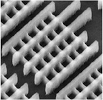
finFETs are vital to the next generation of CMOS processes from Intel, TSMC and others. How will process issues including bulk vs SOI substrates, density limitations, thickness control, and planar device integration affect their practical implementation?
March 28, 2012
Fully depleted silicon on insulator (FD-SOI) transistor architectures may offer speed and power advantages, at the cost of a shift to non-standard substrates.
August 23, 2011
Intel says ‘trigate’—finFET to others—but depleted silicon-on-insulator also has its post 22nm supporters. Chris Edwards reports on the debate at 2011’s Semicon West.


