Critical tools for 20nm design
A look at the way in which key tools, in IC implementation, modeling and extraction, and physical verification, are developing in response to the challenges of 20nm design
The shift to 20nm processes is expected to halve the area used to put a given function on chip, and to offer designers a choice of either halving the design’s power consumption or increasing its performance by up to 35% – or some trade-off of these advantages.
Although the ability to work with more than 20 billion transistors on a die offers huge opportunities, actually doing the design will be more complex than ever. The 20nm process node introduces challenges including possible shifts to insulated substrates (SOI), 3D transistor structures (finFETs) that limit drive flexibility, new middle-of-line (MOL) local interconnections, increasingly complex design rules, and layout-dependent effects.
The abstractions provided by cell-library designers and place-and-route tool developers will hide many of these issues from most designers. It remains a challenge to reduce the impact of increasing design size and complexity on productivity and overall design times. EDA companies are updating key tools in the design flow to meet these challenges.
Physical implementation with standard cells
One of the biggest technological challenges of 20nm processes is the use of double-patterning techniques to successfully pattern critical layers. In double patterning, the most tightly packed features (for example, adjacent Metal One lines spaced at 64nm) have to be split onto two masks so they can be patterned successfully using current lithography.
This means that place and route tools must be able to generate layouts in which each candidate layer can be split (‘decomposed’) into a pair of alternating patterns – without too much impact on the design’s performance and area.
How do you achieve this? The key is to create a layout whose features can be assigned one of two ‘colors’ so that closely adjacent features have different colors – just like in map making.
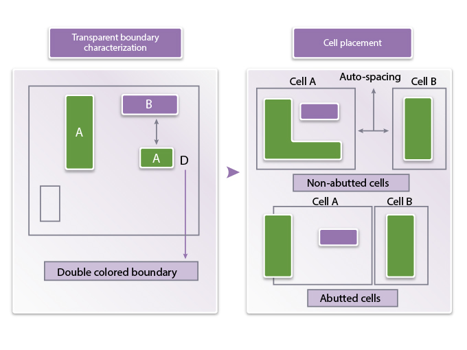
In a ‘divide and conquer’ approach, the place and route tools are updated so that they take into account many of the double-patterning rule requirements. A physical-verification tool that includes a foundry-qualified coloring engine is used alongside to check that adjacent cells will meet the coloring rules. It also checks that the placement has not created coloring violations that are only apparent when analyzing large areas of the chip – so-called ‘large cycle’ violations.
The result of this approach is a ‘colorless’ layout, i.e. one that does not make explicit mask-layer assignments, but which has been shown to be colorable. However, designers can assign critical nets or pins to a mask layer, for example to guarantee the timing of a differential pair. The actual splitting of the layout onto two masks (the decomposition) is often left to the foundry, which uses its own criteria, such as yield enhancement, to drive the process.
The goal is a ‘DPT clean’ layout, in which adjacent cells meet the minimum space requirements if the boundaries are the same color, or have been flipped over or substituted with suitable library alternatives in order to remove the coloring violation.
Figure 1
Legalizing placement for DPT compliance (Source: Synopsys – click image to enlarge)
DPT rules lead to a ‘DPT clean’ layout, but applying them blindly can cause the area of the chip to grow beyond what is necessary. Instead the router needs to apply DPT rules intelligently, for example using spacing rules selectively and knowing when to apply each rule, and when to turn to other techniques.
Coupling these techniques with a physical verification tool that can be used during design helps achieve sign-off in fewer iterations.
Modeling and extraction
The shift to 20nm processes introduces new physical features to chip design, such as the MOL structures used to enrich local interconnect. It is important to be able to model and extract these features in a timely fashion so that their parasitic effects, and therefore the impact they will have on timing in the final silicon, can be simulated.
Double patterning introduces additional variability in both front-end-of-line (FEOL) and back-end-of-line (BEOL) manufacturing due to mask misalignment. The two masks can shift in both the x and/or the y direction, causing spacing and hence coupling capacitance variations that could have a detrimental effect on the performance of critical nets.
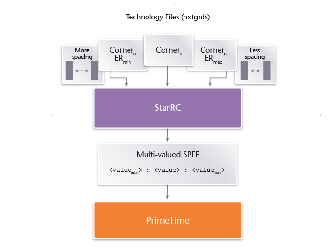
Existing parasitic extraction tools can account for these critical lateral capacitance variations through silicon-calibrated models that include additional process or RC (resistance/capacitance) extraction corners, but this leads to additional extraction and static-timing analysis runs to cover the extra design corners.
Tools that can extract multiple design corners in one run, to create multi-value SPEF (Standard Parasitic Extraction Format) netlists that include minimum and maximum capacitances for a net, can reduce this issue. This only makes sense if the static timing analysis and sign-off tools can use multi-value SPEF files in their analysis runs.
Figure 2
Capturing multi-value SPEF netlists and running them through static timing analysis helps reduce the productivity impact of double-patterning variations (Source: Synopsys – click image to enlarge)
In addition to modeling mask-shift variations, it’s useful for the tools to be able to extract accurate capacitance values for any interconnects that designers have defined as being patterned from the same mask, in order to check that they will meet intended timing. Good pattern matching and 3D extraction algorithms are needed to do the accurate extraction, analysis and sign-off of such designs in a timely fashion.
Physical verification
Physical verification tools need to be updated to handle both the increased density and greater complexity of 20nm processes, through greater exploitation of computer parallelism and more powerful analysis capabilities.
Why is this? The rule-sets that the foundries provide to enable design rule checking (DRC) are becoming more complex. The introduction of double patterning means that the tools now have to increase the area of the chip they analyze in order to find the subtle design rule violations it can cause. The increased use of dummy fill for planarization is increasing the total number of patterns that have to be analyzed.
Advanced pattern-matching capabilities can detect structures in the design that are known to affect manufacturing yields. Strong links between the TCAD process-simulation tools that identify these problematic patterns, or the yield-management tools used by the foundries, help the physical verification tools improve yields. Property and equation-based techniques also help check conformity to foundry rules.
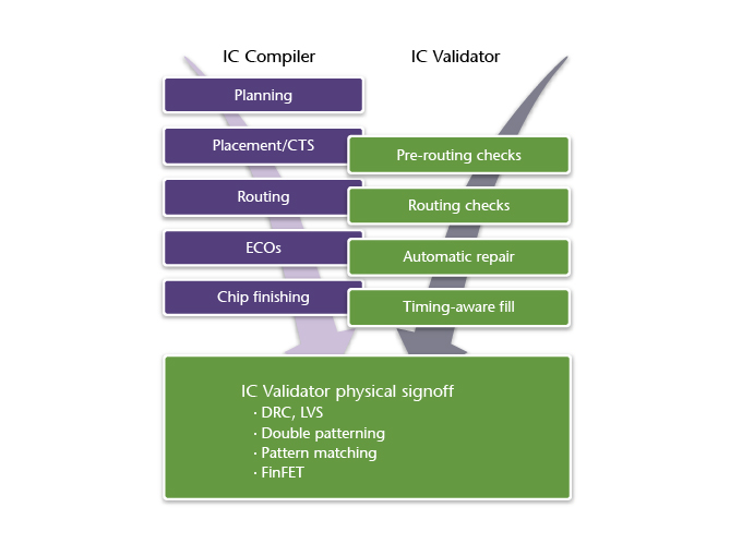
Integrating physical validation tools so that they run alongside place and route tools can help designers avoid issues such as double-patterning violations early on.
Figure 3
Integrating physical checks during place and route can catch issues early (Source: Synopsys – click image to enlarge)
Running a physical verification tool alongside the place and route tool, rather than embodying all the design rules within it, avoids over-constraining placement and routing decisions and so causing the area increases discussed previously. Making physical verification checks a regular part of the design process, rather than relying on rules-based placement and routing until the design is finalized, creates repeated opportunities to find conflicts or rule violations that are occurring at a chip level, or across hierarchical boundaries.
The physical verification tool also provides the relative coloring information that the extraction tool needs to calculate the coupling effects between layout features.
Conclusions
The shift to 20nm processes introduces a series of technological and organizational challenges. The tool enhancements discussed here, along with improvements in other parts of the design flow, will help overcome the technological challenges. Many tools are also being enhanced to address the capacity issue, through better code and/or increased use of parallelism. The combination of technological and capacity enhancement will ease the organizational challenges of producing such large designs.
Author
Andy Biddle joined Synopsys in April 2012 through the Magma acquisition. He is currently a product marketing manager in the Implementation Group, responsible for marketing the Galaxy Implementation Platform for advanced technologies. Andy has more than 30 years of experience in the semiconductor industry, with the last five years in EDA. He has held a number of senior positions including ASIC design, sales, business development, strategic marketing and product marketing. Andy holds a Bachelor of Science in Electrical and Electronic Engineering from London South Bank University.
Links
Find out more about Synopsys’s 20nm offering here
Synopsys
700 East Middlefield RoadMountain View, CA 94043
Phone: (650) 584-5000 or
(800) 541-7737


Hello sir,
20nm technology use in all EDA tools?
Kashyap, could you clarify your question please?