Monolithic 3DIC for SoC
Although production has begun on stacked-die 3DIC products, research is continuing into monolithic 3DIC alternatives as they may over time offer better cost and performance tradeoffs as long as key manufacturing challenges can be overcome. Other than flash memories, monolithic 3D has yet to receive the level of investment seen for stacked-die integration but a series of research projects over the past decade have encouraged chipmakers such as Qualcomm and Samsung Electronics to take the idea seriously as a way of continuing Moore’s Law scaling for SoCs.
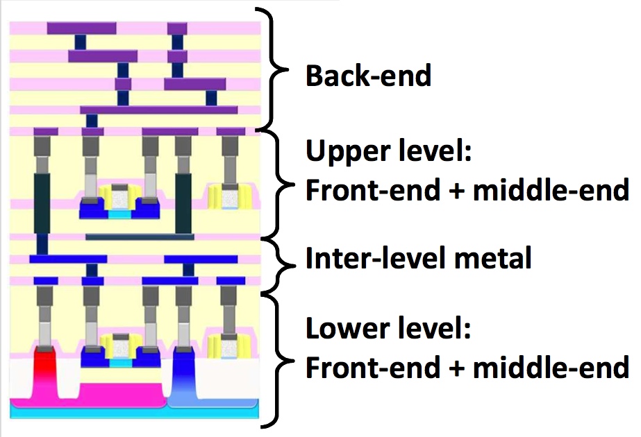
Image Possible implementation of monolithic 3DIC (Source: CEA-Leti)
There are two approaches to monolithic 3DIC that researchers see as viable. One is epitaxial growth, depositing a fresh layer of silicon on top of interlayer dielectric to form a new surface for active devices. The other is to transfer a layer of high-quality of silicon or even completed devices from a sacrificial wafer onto the primary wafer. IBM demonstrated the feasibility of transferring completed device layers more than a decade ago at the 2002 International Electron Device Meeting, then working with a 130nm planar SOI CMOS technology.
Research institute CEA-Leti and Monolithic 3D have developed techniques for transfer of silicon layers that are then processed in situ. Wafer bonding – albeit in readymade wafers from specialist Soitec – is already a key feature of the FD-SOI process developed by the institute and STMicroelectronics. CEA-Leti claims the alignment accuracy of this layer-transfer process is close to two orders of magnitude better than die-stacking techniques that use through-silicon vias (TSVs) as it relies on the accuracy of lithographic equipment rather than the layer transfer and bonding equipment.
Although registration is better than completed layer transfer, a key problem with forming devices above the surface is thermal compatibility. To avoid damaging finished active devices, the back-end-of-line (BEOL) process steps used to deposit metal interconnect are performed at lower temperatures, up to around 650°C, than the 1000°C-plus that can be used in the front-end transistor-fabrication stages. Transistors grown in the metal stack cannot use the same high-temperature processing and annealing steps as those used for base-layer devices – making it difficult to match properties between the upper-layer and base-layer devices unless – unless different annealing processes are applied.
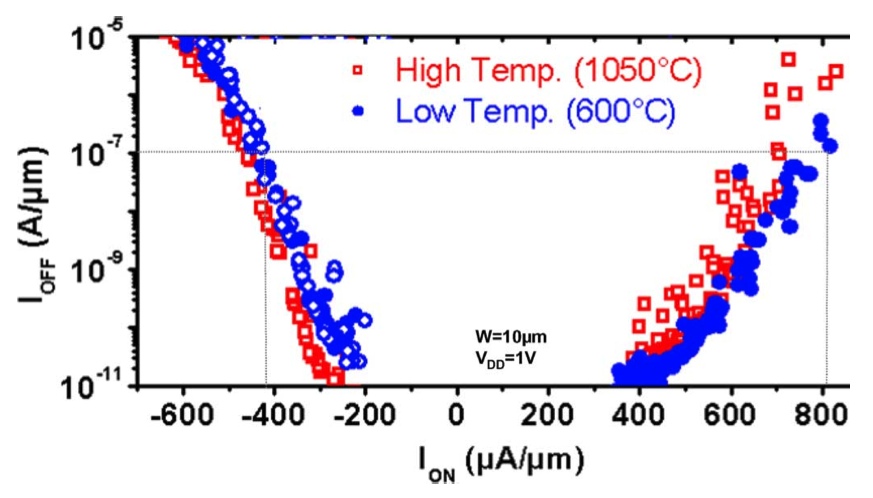
Image Drive and leakage current results for two different transistor layers (Source: CEA-Leti)
CEA-Leti’s technique uses solid-phase epitaxy in place of thermal dopant activation for upper-layer transistors, claiming that the altered technique still results in comparable performance in terms of drive and leakage current for the upper- and base-layer devices. However, the temperatures required damage the copper wiring that may be needed between layers – these can only handle heat up to around 400°C. CEA-Leti is looking at the possibility of using laser annealing or microwave annealing to localize the heating effect – a technique used on epitaxially grown 3DICs.
Towards the end of 2013, CEA-Leti and Qualcomm Technologies signed a deal in which the mobile-SoC maker could gain access to the French research institute’s technology to assess its feasibility.
Samsung has worked on epitaxially grown layers for a number of years. In 2009, researchers at the Korean company developed a 72Mbit multilayer SRAM, with the six transistors of each cell split across three layers. Load PMOS FETs were placed on the second layer and NMOS pass transistors used for access on the top layer. Using a process geometry of 100nm, the cell area covered 0.36µm2, a little over a third of that of a typical 90nm 2D process and comparable to the area taken up by a 40nm or 45nm technology.
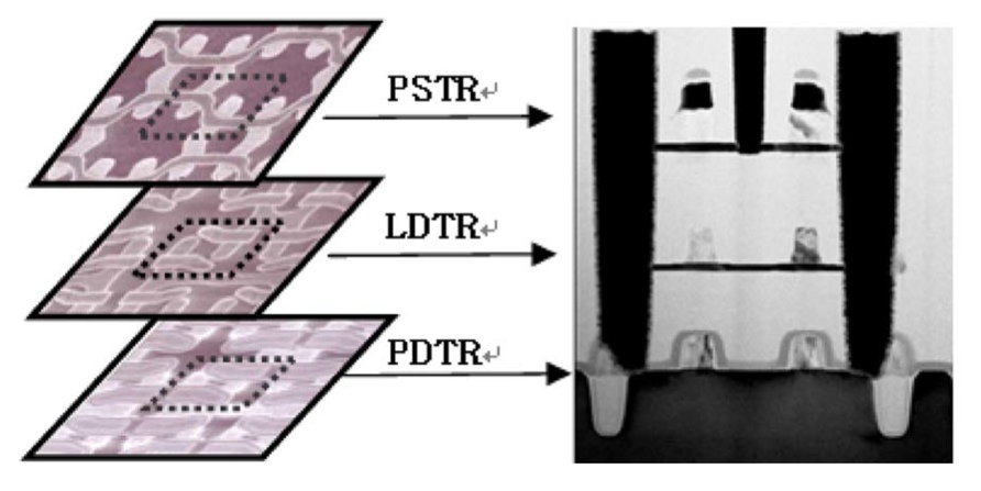
Image SRAM cell divided across three layers (Source: Samsung)
The Samsung process works by growing seed crystals of silicon in contact holes lying within a field of insulators. The contact holes reach down to the base silicon layer, allowing them to grow from the substrate. A layer of amorphous silicon is grown on top of the oxide and silicon surface. The seeds then influence recrystallization after laser annealing is used to melt and reform the silicon layer. Protusions form where the crystals grown around each contact meet but these can be removed using the same chemical-mechanical polishing (CMP) techniques as those used to planarize metal layers. A downside of the seed-window is that the space it consumes eats into overall density.
Technology developed at TU Delft also uses laser annealing to convert a amorphous silicon into a single-crystal form to produce thin-film transistors with mobility comparable to that found in bulk-silicon processes. Although potentially compatible with conventional front-end silicon processes, the current direction of the research is for 3D circuits that can be fabricated on substrates such as glass or plastic.
Compatible transistors
Because of the need to isolate devices, transistors designed for SOI processes are likely to prove the best candidates for monolithic 3D, although this could equally apply to FD-SOI as to finFET. CEA-Leti’s approach focuses on silicon-on-insulator (SOI) devices. With routing layers sitting directly underneath the buried oxide, applying body-bias voltages to tune the performance of the transistors could be expensive to implement – removing one of the key advantages of FD-SOI over a finFET structure.
FinFETs benefit from being made on an SOI substrate as it allows the bottom of the fin to be better defined, which reduces variability. However, planar FD-SOI structures could be applied to post-silicon technologies. Professor Chenming Hu of the University of California at Berkeley believes molybenum disulphide and similar materials would fit neatly into a planar FD-SOI transistor technology and the Berkeley SPICE model for SOI devices can be extended to simulate these structures.
Partitioning choices
Researchers at the Georgia Institute of Technology who have worked on possible design methodologies for monolithic 3DICs have identified three major ways to split functions across layers: transistor-level; gate-level; and block-level. The first to emerge was transistor-level monolithic, used to split PMOS and NMOS devices onto separate layers. This was used in both IBM’s original layer-transfer technology and in Samsung’s 3D-SRAM.
Using separate layers for different types of transistor makes it possible to optimize the materials for each type of transistor, such as channel material and crystal orientation, as well as the gate stack. One of the subsequent experiments performed by IBM on its layer-transfer technology was to rotate the crystal lattice on the donor wafer to boost the mobility of PMOS transistors fabricated onto it.
Gate-level monolithic 3D puts has both types of CMOS transistor on each level and instead distributes standard cells across the tiers. Typically, the metal interconnect that lies between layers is used primarily to wire transistors together within each cell, with the metal layers above the active section employed for intercell routing, except for near-neighbor connections.
Although it has received less attention, work at Georgia has indicated that block-level monolithic 3D, in which the layers carry different IP cores, may be the simplest to work with for design teams coming from a 2D background and should scale readily from techniques that may be used in the future to stack multiple logic dice using TSVs. Comparatively simple tweaks to existing tools are needed according to the researchers. However, it is unclear how tools will deal with the need to route through upper-layer blocks in order to reach global routing layers as well as achieve sufficient connections for power and ground. Blocks may need to be restricted to be members of the same power islands to be able to be placed over one another.
On the other hand, block-level distribution would make it possible to place IP cores according to their need for functions such as body bias. High-performance blocks that need forward body bias for speed or cores that need leakage control so that they can be active for long periods of time, could be placed on the base layer where well-biasing is available. Less critical blocks could be placed on upper layers, potentially relieving the need for those transistors to made with the same levels of drive current and leakage.
Scaling issues
A potential downside of monolithic 3DIC may be lack of further scalability beyond the few layers used in initial processes. Even if manufacturable, there is no guarantee that a viable architecture for a two-layer stack will translate neatly into one that uses three as the interlayer routing requirements may prove to be different enough to warrant large-scale changes. For example, if the first generation of the process overlays PMOS transistors on top of NMOS, it is unclear what role the third layer would play in that scheme, perhaps calling for a shift to an architecture in which NMOS and PMOS again share a layer and the interlayer is used to route between single-layer standard cells instead of highly local routing within a multilayer standard cell.
Focusing on different elements of an SoC may lead to different solutions. For example, by concentrating efforts on a regular 3D SRAM structure, most SoCs would achieve further scaling benefits even if logic does not scale by the same amount as the SRAM. Such an approach would probably favor a shift back to stacked-die architectures in which memories are separated out from the core SoC and optimized for manufacturability on their own.
As with stacked-die structures, heat removal is an issue for monolithic 3DICs. One possibility is to use some of the interlayer vias as heat pipes to aid thermal conduction – the seed windows used in epitaxially grown 3DICs could conceivably be etched in a similar manner as TSVs and replaced with a high thermal-conductivity material. Work by researchers at Stanford University has indicated that the power-delivery network itself might be harnessed as a way of distributing internal heat to the package.
