Transistor stacks piled high at VLSI
As 2D scaling becomes increasingly difficult, researchers reporting at VLSI Symposia have focused attention on what can be done in the third dimensions to improve density and performance without a sudden break from conventional CMOS processes.
In one experiment presented at the first virtual VLSI Symposia this week (June 15, 2020), a team from CEA-Leti has shown that it is possible to construct nanosheet-based transistors with as many as seven vertically stacked in order to boost the current drive of nanometer-scale devices. Researcher Sylvain Barraud said stacked nanosheets provide a way to maximize the “fin effect” of using parallel channel fins without increasing the area footprint of transistors.
The nanosheet gate-all-around (GAA) construction provides a way to reuse the extensive process work done on finFETs by pushing effective channel width into the third dimension. Barraud said the rotation of the fins so they are parallel with the wafer surface also provides the ability to tune sheet width itself during design in a manner that was not available for fin height with conventional finFETs. In the work presented at VLSI, the team experimented with sheets as narrow as 15nm and up to 85nm wide.
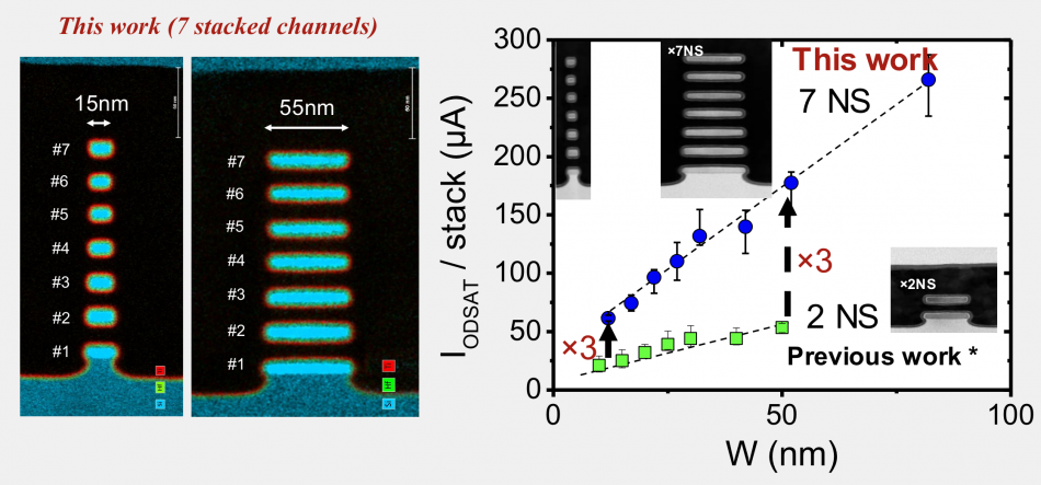
Image Drive current enhancement of seven-layer nanosheet transistor
The team found having more sheets in a single stack rather than a smaller number in a dual stack maximized the “nanosheet effect”, an improvement in performance analogous to the fin effect in finFETs. Although it increases process complexity, the payoff comes in improved performance.
“The result is a drain-current enhancement that is proportional to the effective width increase,” Barraud said.
Compared to a prior projects with two stacked nanosheets, the drain current was increased threefold for the same sheet width. Increasing the width from 55nm to 85nm boosted the current through the stack by around another 60 per cent.
Barraud said more work is needed to investigate effects such as self-heating with a large number of stacked channels as the increased current may lead to large changes in temperature as the device is switched that prove harder to deal with than with transistors that support lower drain currents though the larger number of channels may reduce the self-heating effect for a given current. “We will have to find a good tradeoff between heat generation and dissipation,” he said.
Buried power
Continuing work unveiled at VLSI Symposia two years, Anshul Gupta of Imec described a project to assess the manufacturability of buried power rails and their effect on the performance of transistors built over them. Buried power rails provide a mechanism for reducing the area of standard cells by allowing more of the lower metal lines to be used for logic routing between transistors. Power can be dropped into cells using a smaller number of metal vias by routing them under the silicon surface. There is even the potential for power to be supplied from the backside of the chip and remove the need for extensive power and ground meshes in the upper metal stack.
Work on the overall architecture found there is sufficient space in shallow-trench isolation regions around cells to route the power rails without them having to pass underneath transistors directly, which minimises stress caused by the metal insertion within the silicon surface. Also, encapsulation using silicon dioxide plugs helps avoid the risk of metal contamination during front-end processing. “We found the buried power rail does not degrade CMOS performance,” Gupta claimed.
For the rail itself, tungsten is the primary metal for carrying current with ruthenium chosen to act as the main material for vias that connect the buried rails to the power distribution grid connections at M0.
Junctionless 3D
A further option for moving into the third dimension is to deposit secondary layers of transistors on top of the main layer. A lingering problem is one of thermal budget as the high-temperature processing need to form full CMOS transistors in a secondary layer may compromise those already formed underneath. A compromise is the junctionless transistor, which can be made using less heat-intensive process steps. Performance of these junctionless transistors will be lower but they might be employed for low-speed and I/O circuitry.
“For analog applications, variability is a big issue,” said Daphnée Bosch of CEA-Leti, who described work by her and colleagues to investigate these issues with 18nm gate-length devices on thin-film SOI. They found the use of back-bias control helps reduce the effects of variability though it is also sensitive to thickness variation of the silicon channel. High control over both may be needed to make junctionless devices practical for monolithic 3D architectures.