EDA in the cloud boosts DRC iterations for AMD
In a recent collaboration between AMD and Microsoft Azure, the chip company was able to increase its design-rule check iterations on a 7nm full reticle design from 1-1.5 times a day based on internal resources, to 3 times a day by transitioning to running DRC EDA in the cloud.
Further cooperation on best practice to optimize for cloud-based physical verification was provided by AMD’s EDA vendor Mentor for the Calibre tool family. This further reduced individual runtimes for DRC by three hours.
The whys and wherefores behind these efficiencies are considered in ‘EDA in the cloud‘, a white paper from Mentor, a Siemens business.
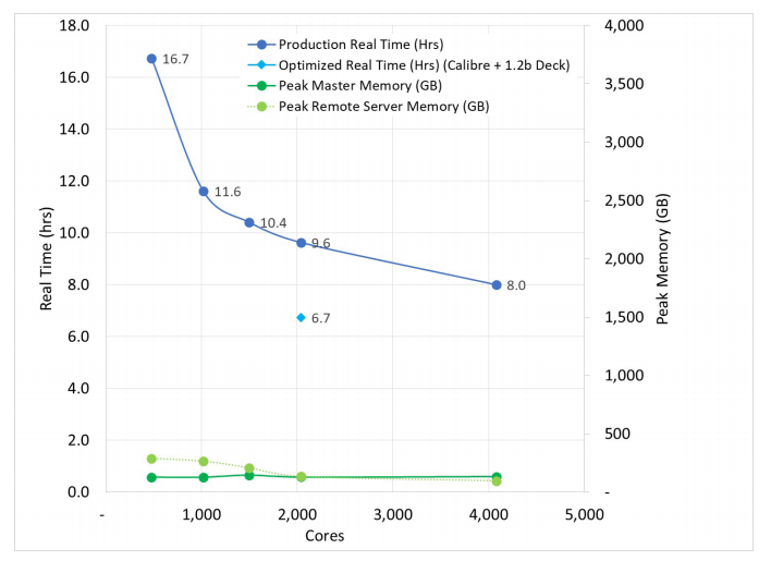
Figure 1. AMD cut DRC run time and controlled memory usage with EDA in the cloud (AMD/Microsoft/Mentor)
The paper considers how the key security concern over cloud-based design has been addressed by providers that can now typically provide better IP protections than any company could on its own. But a more important factor may be the ramping compute demands posed beyond 5nm.
EDA in the cloud toward and beyond 5nm
Author Michael White notes that each progressive node has typically required a 20-30% increase in compute resources. Already, the industry has already moved from running designs across 10s of cores to 100s. In addition, the future is beginning to pose a series of new, more complex challenges in terms of how traditional steps are taken.
“Fast-forward to the 5nm node, and DRC is not just DRC. It’s DRC, equation-based DRC, multi-patterning, and pattern matching. LVS [layout vs schematic] is not just LVS; it’s LVS plus advanced device parameters, such as electrostatic discharge checking and reliability checking. Fill no longer means simply adding in a few geometries; now design companies are trying to maximize fill using techniques like cell-based fill,” White writes.
“All of those changes mean that not only has the number of checks gone up, but the types of checks have expanded, and the number of check operations has grown drastically.”
Meanwhile, lithography is evolving towards techniques such as numerical aperture EUV (NA-EUV); there are new transistor types such as gate-all-around (GAA); and 3D packaging such as small outline IC (SOIC) is on the agenda.
In this context, EDA in the cloud is proving powerful not just in terms of meeting the extra compute demand but also, as White explains, shrinking time-to-market, with the latter now becoming more of an attraction that server cost.
The paper, which is available for immediate download, considers these issues in more detail and includes a link to an accompanying video on the AMD-Azure collaboration.