Chipmaking’s new environment presented at IEDM
In his keynote at the International Electron Device Meeting (IEDM) on Monday, Imec senior vice president of CMOS technologies Sri Samavedam outlined the likely roadmap the monolithic chipmaking technology will likely follow in the decade to 2030 and a possible switch from silicon transistors to devices based on 2D material such as MoS2.
Process implementors and designers will have to face a growing number of tradeoffs as concerns such as environmental sustainability enter the picture. The immense energy consumption of EUV scanners used for lithography as well as exhaust gases from etching and other chemical treatments needed for ever more complex front-end and back-of-line (BEOL) processes are bringing a focus on how big the carbon footprint chipmaking is. However, the tradeoffs are far from obvious.
Samavedam used comparisons of EUV and self-aligned quadruple patterning (SAQP) based purely on immersion lithography to show the complexity of the problem. With EUV there is a clear dependence on wafer throughput because of the energy consumption of the laser source. Whereas SAQP may consume as little as half the electrical energy of a low-throughput EUV line, producing just 40 wafers per hour. The EUV line begins to win at 100 wafers per hour based on Imec’s calculations. Other calculations, to be covered in a separate paper at this week’s conference, focus on highly energy-absorbing gases such as the fluorinated chemicals used for etching.
Environmental framework
“We have developed a framework to evaluate the environmental impact of process flows in the pathfinding phase,” said Samavedam. “We have now also taken the Imec process-cost models to include sustainability metrics like power consumption, ultrapure water consumption and greenhouse gas emissions. This framework creates awareness about environmental impacts and allows fabs to make more sustainable choices early in the technology definition phase.”
However, a big impact on throughput and energy-per-chip will be on the coming changes to EUV-based patterning beyond the 5nm node. “At 3nm we will be at the third generation of EUV. Patterning pitches below 28nm will require multiple exposures,” Samavedam said. It is not clear which technique will win at this stage but the choices are similar to those encountered in the early days of multiple patterning for immersion lithography. Imec is looking at both self-aligned double patterning and a pair of litho-etch cycles. There is even an option for using immersion lithography in a variant of quad patterning that uses two rather than three or four EUV mask steps. That winds up the cheapest option but at the cost of higher variability and defectivity, he noted.
As EUV scanner technology itself improves, a high numerical-aperture (NA) variant may step in towards the end of the decade and help reduce cost and energy by bringing single patterning back for 20nm-24nm pitch lengths, Samavedam added. Even though high-NA tools will be even more expensive, the result would be an estimated cost reduction of 14 per cent compared to multiple-patterning flows.
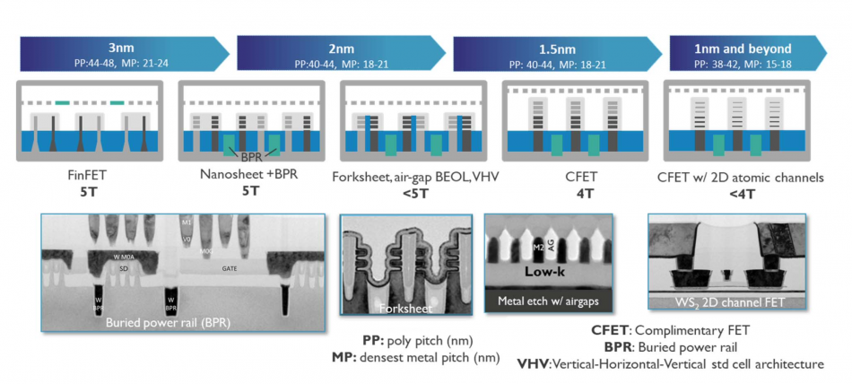
Image Imec's proposed roadmap for scaling to 2030
Pitch scaling, luckily, is not the only way forward. Samavedam pointed to the growing use of 3D structures to increase density as Imec continues to work on stacked device architectures such as the CFET, which places the n-channel and p-channel transistors in an inverter on top of each other. As standard-cell libraries scale down to a height of 5T, performance will suffer because the transistors can use only single fins. Nanosheets provide a way to stack channels on top of each other, overcoming the space problem for high-drive transistors at the expense of a more complex process.
With nanosheets, the isolation region between n- and p-channel devices consumes valuable area so the next stage, allowing sub-5T standard cells, is the proposal of the forksheet, which brings the two channel together and uses the isolation barrier as a self-alignment feature. “But as you scale below 5T you may need new standard-cell architectures such as VHV,” Samavedam says.
The change from conventional horizontal-vertical-horizontal (HVH) routing for intra- and intercell wiring sounds like a simple rotation but for it to improve density as well as cell-pin accessibility, VHV needs an additional middle-of-line (MOL) routing layer.
Another “scaling booster” proposed by Imec is to bury the power lines, a technique proposed along with the CFET a couple of years ago at VLSI Symposia. This will likely be followed by putting the entire power grid on the backside of the die, similar to the way in which power transistors are built today. That could go further Samavedam said by putting metal-in-metal capacitors and other passives into the metal grid.
Beyond the monolithic IC, Samavedam said stacked-chip technologies will become much more important but will need in addition to improvement to interconnect changes to EDA tools to allow the concurrent design of chiplets.