Pillar transistor points to smaller SRAMs at 5nm
Research institute Imec and Singapore-based Unisantis Electronics have developed a process flow based on a vertical transistor with a gate on all sides they claim will lead to denser memories on a 5nm node.
In the jointly developed process, the Surrounding Gate Transistor (SGT) developed by Unisantis is intended to lead to a 6T-SRAM cell with an area between 0.0184 and 0.0205µm2. Imec claims the vertical-gate transistor allows for cells with a 20-30 per cent reduced area compared to horizontal gate-all-around (GAA) FETs and offers lower operating voltage, standby leakage, and improved stability. Unisantis sees the gate as being suitable for DRAM and flash cells as well as SRAM.
“SGTs have all the advantages of horizontal gate-all-around transistors, allowing a near-perfect electrostatic control of the transistor channel,” said Professor Fujio Masuoka, director and CTO at Unisantis and inventor of the SGT concept. “But because the channel is a vertical pillar, the concept has the potential for a significant area reduction compared to horizontal nanowire-based transistors.”
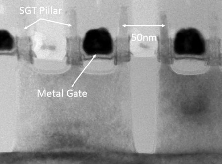
Image Cross-section of an SRAM cell based on the SGT structure
The researchers on the joint team used a design/process-technology co-optimization (DTCO) procedure to develop the SRAM’s core transistor and surrounding circuitry. It led to a layout with an area of 0.0205µm2 based on a minimum pillar pitch of 50nm. Imec claimed this is a 24 percent improvement on the scaling factor of SRAM architectures published to date and is ready for an N5 or 5nm technology node.
One of the problems the team had to deal with was the mechanical stability of the pillars at the high aspect ratios that were required. Imec said the use single-exposure EUV lithography would keep the number of process steps to minimum and lead to a production cost comparable to that of finFET-based SRAMs.
