Imec cuts transistor gap to less than 20nm with forksheets
Imec described at this week’s VLSI Symposia on Technology and Circuits (June 15, 2021) a process flow that would yield a denser form of nanosheet transistor that might act as a successor to those being introduced by the foundries in the N3/3nm and N2/2nm nodes.
Using a form of self-aligned double patterning (SADP) tweaked in a way that process engineers normally avoid, the Imec team managed to reduce the gap between complementary NMOS and PMOS nanosheet devices, each with its own work function metal stack, to just 17nm. ”To my knowledge, it’s the first time that dual work-function metal has been demonstrated at such a low spacing,” claimed Hans Mertens, principal member of technical staff.
The research institute originally proposed the forksheet structure at the 2019 International Electron Device Meeting (IEDM). “The forksheet FET is a particular type of nanosheet device that allows aggressive scaling of the space between N and P devices and therefore provides area-scaling potential,” Mertens said.
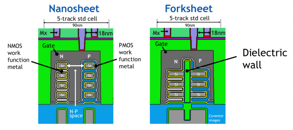
Image The dielectric wall of the forksheet allows for tighter spacing between NMOS and PMOS
The key to the forksheet structure is an insulating wall, in this case silicon nitride, between two parallel transistors. It turns out that this wall comes with a number of benefits and one drawback. Because of the need for different work-function metals for the NMOS and PMOS transistors, there is a limit on how closely spaced conventional nanosheet device can be in a cell such as an inverter. A problem that emerged in experiments with gate-all-around (GAA) nanosheet construction is that the steps used to deposit the NMOS gate materials results in part of the gate on nearby PMOS devices being undercut. There is also a problem caused by the high aspect ratio of the mask used to separate the two types of transistor during the replacement metal gate process fabs expect to use.
The fins out of which the nanosheets are formed are patterned using SADP using a form of “pitch walk” detuning that puts the second fin much closer to its neighbour than would be the case for conventional SADP where the emphasis is on maintaining a as consistent a spacing as possible. That is followed by a conformal coating of silicon nitride that is etched away from everywhere except the narrow 20nm gap between paired fins. After that, nanosheets are cut out by etching away the silicon germanium, ready for the metal-gate deposition stage.
The process flow allows for unpaired transistors so standard-cell designers and others can have greater flexibility. “You can have nanosheet-only structures with a spacing of 40nm where this wider spacing is needed,” Mertens said.
The wall turned out to provide a degree of assistance for gate formation as it results in a lower aspect ratio for the mask by allowing part of it to rest on the top of the wall. The wall also prevents over-etching of the PMOS gate, which is formed first, by the NMOS processes. Because the wall allows the gap between transistors to be reduced further than with conventional nanosheet processing, the payoff with a standard cell that has the same track height comes in a wider transistor with higher drive strength. Mertens said in this experiment, the effective width of each forksheet device could be 21nm compared with 12nm for a purely nanosheet-based process.
The result is better power-performance curves as well as lower capacitance between the transistors. However, the potential disadvantage of the forksheet is harder to see in this experiment. Compared to N3-class finFETs, the device has a relatively long gate of more than 20nm. This is exacerbated by some properties of the process that lead to a longer effective gate length. Mertens said some process optimizations to form recesses in the insulating wall would help reduce this gate-length expansion. The result is that the experiment does not demonstrate an expected worsening in subthreshold slope in moving back from a GAA to a trigate channel. “A shorter gate is needed to detect the differences,” Mertens said.