Nanometer scaling puts focus on power at VLSI in June
At the upcoming Symposia on VLSI Technology & Circuits, the first to be held online, engineers from Qualcomm will describe an adaptive clocking scheme to cope with short-term power fluctuations and operate a processor much closer to its voltage margins.
The work, performed in cooperation with University of Texas, is on a digital signal processor implemented on a digital signal processor (DSP). Many previous approaches to adaptive clocking where the timing of the circuitry is very sensitive to changes in voltage and available power have focused on reacting rerunning cycles when a voltage droop pushes operation past its safe margin. This research uses microarchitectural signals coupled with a power model to anticipate surges in demand for power and slowing the clock temporarily to account for problems caused by voltage droop. The authors claim a benefit of a 10 per cent higher clock frequency or a corresponding reduction in supply voltage.
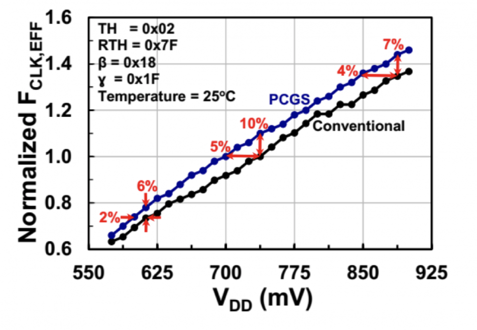
Image Improvement in clock frequency against Vdd with Qualcomm's adaptive clock
A paper from Imec focuses on another aspect of deep scaling: the need to improve density when gate and metal scaling becomes much more difficult to achieve. The Imec researchers described their work on buried power rails two years ago to remove the overhead of conventional supply delivery networks in sub-5nm processes. Their upcoming paper at VLSI will demonstrate the integration of tungsten buried power rails with silicon FinFETs. They found the characteristics of CMOS in close proximity to floating buried lines to be similar to the characteristics of CMOS with conventional power rails. Combining tungsten with ruthenium for the via contacts showed the architecture can withstand more than 320 hours of electromigration stress at 4MA/cm2 and 330°C, pointing to the metal as a good candidate for via metallization to achieve a low resistance contact strategy for buried power rails.
Another feature of sub-7nm processes is the likely move to gate-all-around (GAA) transistors based on nanosheets. At VLSI researchers from a team at CEA-Leti Minatic will describe the tradeoff of using multiple sheets to increase the effective width for a given areal footprint against process complexity. Their experiments have indicated that a seven-level stacked nanosheet design can provide a three-fold improvement in drain current over simpler two-level stacks together with a high current drivability of 3mA/μm at a 1V supply voltage.
More than a decade ago, IBM showed how air spacers in the metal interconnect could cut parasitic capacitance. At this year’s conference, the gap has moved down into the transistor layer. The IBM researchers will report an improved air spacer that is can be co-integrated with finFET transistors in a self-aligned process. According to the team, the integration scheme enables air spacer formation agnostic to the underlying transistor architecture so that the spacer could be used not just with finFET but GAA transistors. The experiments with a finFET showed a 15 per cent reduction in effective capacitance. According to IBM, the power/performance benefits achieved by the new air spacer exceed the benefits of scaling a finFET from 7nm to 5nm.
Having over the years worked on a number of techniques to combine III-V materials and transistor architectures with CMOS, Intel will talk about work to bring the power-handling benefits of gallium nitride (GaN) to a CMOS silicon. The work uses layer transfer to combine high-speed silicon finFET devices on a (100) substrate with a variety of analog- and power-oriented GaN transistors on a high-resistivity Si(111) wafer. The GaN devices include enhancement and depletion mode transistors with drain current density up to 1.8mA/μm.
The 2020 VLSI Symposia in mid-June will see the conference celebrate its 40th year and has taken on the theme of “The Next 40 Years of VLSI for Ubiquitous Intelligence”. The week-long virtual conference will feature of technical presentations, plenary sessions, panel discussions, joint focus sessions, and short courses presented in an online format.
The Symposia will have two technology plenary sessions. The first session on June 15th will feature “5G Evolution and 6G,” by Takehiro Nakamura, senior vice president & general manager of 5G Laboratories at NTT Docomo, and “Silicon is Greener: Why Innovation in Circuits is Needed for Sustainability,” by Jen Lloyd, vice president for the precision technology and platforms group at Analog Devices.
The second plenary session on June 17th will have the talks: “The Future of Compute: How the Data Transformation is Reshaping VLSI,” by Michael Mayberry, chief technology officer at Intel; and “Empowering Next-Generation Applications through flash Innovation” by Shigeo Ohshima, technology executive at Kioxia.