2D advances to take center stage at IEDM
This year’s International Electron Device Meeting (IEDM) will feature a number of advances in the use of 2D materials for future high-integration logics as well as novel integration schemes for power and other specialist semiconductors.
At the conference in San Francisco in early December, a team led by TSMC engineers will describe how they obtained almost ideal subthreshold-swing behavior from a monolayer of molybdenum disulfide (MoS2). Using hafnium-based dielectrics similar to those already used in silicon fabrication, placed using atomic-layer deposition on top of the monolayer, the engineers built a top-gate FET with a subthreshold swing of less than 70mV/dec. In doing so, the team overcame a number of the prior issues of building 2D-material transistors, which make it difficult to deposit pinhole-free dielectrics.
Another TSMC-led group worked on ways to implement 2D-based devices using similar gate-all-around (GAAs) structures to those now being developed for silicon transistors. The team will describe at IEDM a possible integration flow for 2D monolayer devices based on transition metal dichalcogenides such as MoS2. As part of the work, they built a demonstration device with a gate length of 40nm and a channel just 0.7nm thick that was able to deliver on-current of around 410µA/µm at a supply voltage of 1V. The on-off current ratio was found to be more than 108 with almost zero drain-induced barrier lowering. Higher drive currents should be possible by stacking channels, as with the nanosheets being prepared for silicon processes.
Though they offer high internal conductance, one issue with 2D materials has been that of contact resistance, particularly for p-channel devices. Working with universities in Japan and the US, TSMC has worked on ways to reduce the Schottky barrier. Computational modeling provided a number of options that could potentially act as p-type contacts to tungsten selenide (WSe2), including materials known as semimetals that have differing degrees of conductivity based on paths through the material that carriers can take. Others are simpler metallic contacts such as a form of titanium sulfide. In some, the contact resistance was predicted to be as low as 20Ω.µm and the team has begun physical experiments for further evaluations.
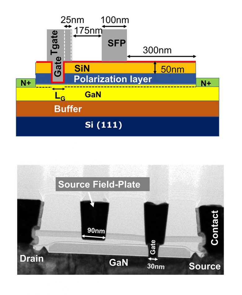
Image Intel engineers put a field plate into a short-channel GaN-on-Si device to control its high electric field
To support the power needs of high-end silicon devices in the shorter term, Intel engineers looked at the possibilities for gallium nitride on silicon, following on from work presented last year. The team scaled the finFET-type devices to a channel length of 30nm and improved performance though the use of a submicron-long source field plate to manage the electrical field within the device. They achieved an operating voltage of 40V and a record Fmax for GaN-on-Si devices of 680GHz.
As thermal management is a major issue in power semiconductors, attention is turning to novel materials for their ability to conduct heat away from active devices. Diamonds is used in some specialist heatsink designs because of its high thermal conductivity. Work by Stanford University and other institutions propose the formation of diamond films around the gates and channels of individual transistors as a possible way mechanism to improve heat flow from individual devices to the larger heatsink. They used a polymer-assisted seeding technique to completely surround a GaN high-mobility transistors with CVD-grown diamond. They found that the diamond-encapsulated transistors had lower peak and average channel temperatures to conventional designs, bringing peak temperatures down by almost 60°C in some cases. They also exhibited fewer hot spots.
Modeling may expose other ways to deal with the heat generation of power semiconductors. An IMEC-led team developed a thermal-modelling frameworks that takes into account the way in which carriers and phonons cannot travel far enough within the transistor’s crystal lattice to diffuse heat in the way that conventional simulations predict. Based on Monte Carlo simulations, they modeled heat flows in GaN and indium phosphide devices and found transistor-level peak temperatures in RF circuits can as much as 70 per cent higher than previously thought. They performed experiments with GaN-on-Si amplifiers to validate the models.
This year, IEDM takes place from December 3rd to 7th, 2022 in San Francisco but will also offer an on-demand service for recorded presentations after the physical conference has ended.