Advanced processes feature at VLSI in June
Among the papers at this year’s VLSI Symposia in Hawaii in June, Samsung will describe a 7nm CMOS process that uses EUV lithography to tighten up device features on minimum-pitch interconnects.
The use of EUV on the 7nm process is expected to reduce the number of mask steps by 30 per cent compared to a process that uses 193nm lithography throughout. According to Samsung, the 7nm process will have around 15 per cent fewer steps than its 10nm predecessor. The company used EUV lithography on the test chips to define middle-of-line (MOL) contacts and minimum-pitch metal interconnects and vias.
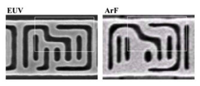
Image Comparison of 7nm cells imaged by Samsung using EUV and 193nm lithography
Researchers from two Taiwanese universities working with UMC will describe an implementation of resistive non-volatile memory (RRAM) on a standard 14nm CMOS finFET platform, using the transistor fins for storage and to suppress sneak paths that afflict this kind of memory.
IBM and CEA-Leti have worked together on the application of InGaAs to FD-SOI for monolithic 3D integration. It combines a short-channel gate-last approach using the III-V material on the upper layer and a more conventional gate-first construction silicon gate on the base layer.
In separate work, IBM and a group of Chinese research organizations have explored the use of germanium for improved mobility on finFETs. IBM claims the approach will support high performance at a supply voltage of 0.5V. The National Nano Device Laboratories working with the National Cheng Kung University and others have combined germanium with a hafnium dioxide-based ferroelectric gate insulator to create a device with a subthreshold slope of 58mV/decade.
