Samsung 7nm uses EUV and split fin widths to push speeds
Fin widths tuned individually for NMOS and PMOS are among the techniques Samsung has used for its 7nm process technology, the company revealed at the recent VLSI Technology Symposium in Kyoto, Japan.
To reduce the number of overall mask steps and improve the definition of some critical layers, Samsung expects to make limited use of extreme ultraviolet (EUV) in place of multiple patterning. The engineering team developing the process opted to use EUV lithography on the middle-of-line (MOL) contacts and on the minimum-pitch metal and via interconnects. The move cut the number of mask steps in the overall process flow by at least a quarter and offers better results, the company claimed.
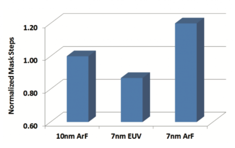
Image Change in number of mask steps needed between double-patterned 10nm and two 7nm process flows
For the 7nm technology, Samsung has made the PMOS fins thinner than the NMOS versions and, compared to 10nm made them with less tapering and with a higher aspect ratio. According to the company, the thinner PMOS fin controls drain-induced barrier lowering (DIBL). The NMOS fin does not suffer the increase in source-drain resistance it would have if it used the same thin-fin structure as the PMOS device.
The process employs a gate-last approach with the use of multiple work-function materials in the gate stack to support three choices of threshold voltage without suffering a degradation in current handling between them.
Samsung said EUV lithography helps cut variation in width and spacing in the minimum-pitch metal interconnects and helps cut the routing congestion that would be caused by the use of multiple vias that would have been needed under double patterning.
The better fidelity of EUV-defined patterns reduced the amount of corner rounding compared to 193nm lithography as well as critical-dimension (CD) variation, the company said. Another benefit is in the elimination of metal dummy and metal cut layers in the EUV-defined layers, so that devices do not suffer from the increased parasitic capacitance caused by those features.
According to Samsung, the 7nm CMOS FinFET supports 20 per cent faster circuit speeds or consume 35 per cent less total power than the 10nm predecessor. Process tuning to keep parasitic and channel resistance down helped improve the ratio of drive current to off-state leakage compared with the 10nm process.