Qualcomm’s take on preserving Moore’s Law economics
Qualcomm’s VP of Technology does not share the same concerns as some of his colleagues as 20nm. However, as Geoffrey Yeap told IEDM 2013 in a keynote address, he is still concerned about what will happen as the industry tries to map the path beyond that. With 7nm – expected around 2017 – requiring some serious innovation if it is not to prove an economic roadblock.
“People complain that there isn’t enough of a performance advantage at 20nm over 28nm, but you can get an extra 12% on top from optimization,” he said. “Also, 20nm paves the way for 16nm finFET. So yes – it’s worth it.”
Beyond that, however, things do get more tricky and Yeap highlighted three areas in particular.
- BEOL RC/area/cost scaling
- Meeting low power operation for days of use
- The ‘mobile SoC scaling box’ (speed*density/power/cost)
Before discussing these in more detail, it is useful to look at how mobile SoC scaling requirements differ from those for traditional CPUs or GPUs, fostered when the PC dominated silicon design.
Mobile’s demands now chart the roadmap, particularly at the foundry level. “Since the 65/45LP nodes, the mobile SoC market has grown extremely rapidly,” said Yeap. “Shipments of smartphones passed global PC shipments in Q4 of 2010 for the first time in history. Tablet shipments are forecast to surpass total PC shipments in the fourth quarter of 2013. We are definitely in the post-PC era.”
The extra elements that mobile impose upon scaling are, as is well known, power and cost. But Yeap summarized some finer distinctions – and that ‘scaling box’ from Qualcomm’s point of view – in a useful chart.
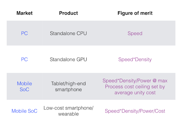
Comparative SoC figures of merit (Source: Qualcomm)
So where do the problems lie and what possible solutions are there?
BEOL
“For the first time, BEOL cost is projected to exceed 50% of the total mobile SoC scaling cost at 10nm,” Yeap said. “The BEOL-gate delay gap widens to more than c1,000X at the 10nm node.”
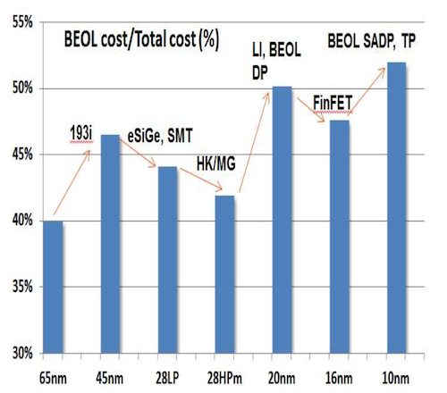
BEOL as a percentage of overall scaling cost (Source: Qualcomm)
Yeap said that there have been just two major BEOL interconnect breakthroughs in the last 15 or so years: Cu/F-TEOS dual damascene interconnects at 0.22um and carbon-doped oxide low-K dielectrics at 90nm. This innovation path now needs to be revisited urgently.
“A breakthrough in BEOL cost/RC scaling can come from fundamental material innovation,” Yeap said, “accomplished through open collaboration among foundries, consortia, tool and materials suppliers and academia.”
In other words, it’s a big job and it needs everybody’s input. Yeap drew a comparison with the work already underway through broad industry groups on next generation lithography and 450mm wafers.
Low-power operation
The consumer does not just expect devices to do ever more, ever better. Qualcomm’s roadmap specifically foresees multi-day operation rather than just standby.
In the short term, finFETs will soon offer some help with sub threshold slope at near the “ideal” level of 60mv/dec. They will reduce Vcc-min.
“However, finFETs also come with higher parasitic capacitance. This may be reduced by larger contacted gate pitch only in certain needed circuit blocks without increasing die area substantially,” Yeap said. “Future transistors need an effective way of using the back gate for asymmetric gate operation and dynamic threshold voltage control while FinFETs lack an easy way to access the back gates.
“This is especially crucial when Vdd continues to scale lower to a point that there is just not sufficient Vg-Vt to yield meaningful drive current.”
At this point, Yeap noted the elephant – or more exactly elephants – that show some promise: FDSOI and ETSOI, though added concern about “ecosystem, capacity and high starting wafer price issues”.
The Qualcomm scaling box
With lithography no longer driving scaling as it once did, each successive node entails materials and device advances, increases in process cost, and an ability to cope with increasing design complexity to pick up the slack. This “positive feedback loop drastically accelerates the increase in die cost” based on $/sq mm. So at what point does this start to make scaling economically unattractive, breaking Moore’s Law for real.
“We are getting dangerously closer to this inflection point as the scaling box with its four sides of speed, density, power and cost becomes smaller as we march towards the 7nm node,” Yeap said.
Here, though, Yeap could offer a raft of options. A critical one is reducing the SPICE/RC model-to-silicon gap.
Already, Qualcomm uses a restricted design rule strategy. Large, always-on, low frequency blocks are designed with cells that include horizontal routing poly and flexible polygon shapes. Meanwhile, variation minimization rules enforce the regularity of poly and active regions to improve the robustness of performance-critical macros and sense amplifier blocks.
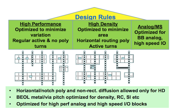
Two-fold RDR strategy to enable high-density and low-variation blocks in a mobile SoC (Source: Qualcomm)
This, however, does not optimize the outcome as much as Qualcomm would like. Again, more collaboration and better models (and less pessimism) are needed.
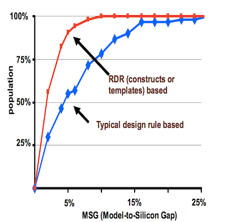
Model-to-silicon gap (Source: Qualcomm)
Beyond that, Yeap noted that he still feels upbeat about integration, starting with options such as 2.5D interposer, 3D through-silicon-via, and fan-out wafer-level packages, then moving on to monolithic 3D integration. He also noted advancing research in not only finFETs but also silicon germanium and other three-fives, gallium arsenide and tunneling FETs.
He concluded by repeating the need for greater collaboration and proposing that the whole industry goes on a fairly radical diet.
- Zero cost increases (cut out the cholesterol)
- Zero design pessimism (cut out the fat)
- Zero model-to-silicon gaps (cut out the MSG).