Samsung couples EUV with DTCO for 7nm shrink
Samsung Electronics expects to increase savings on die area in the shift from its 10nm to 7nm node by applying both EUV for critical layers and several layout-focused process changes.
Samsung researcher WonCheol Jeong explained at the VLSI Technology Symposium this week (20 June, 2018) that for critical layers such as the lowest metal routing the company wants to move away from multiple patterning, which may have demanded as many as five masks for a single layer, because it causes too many problems for design and yield.
“EUV shows superior pattern fidelity. It could give higher yield, shorter turnaround time and, ultimately, lower cost,” Jeong said, adding that the die area based on a combination of scaled contacted poly pitch (CPP) and metal spacing should be 40 per cent that of a device made on 10nm. The shift to EUV will let Samsung tighten the critical dimension (CD) distribution. “CD distribution could be better by 1.6x compared to SADP,” he said.
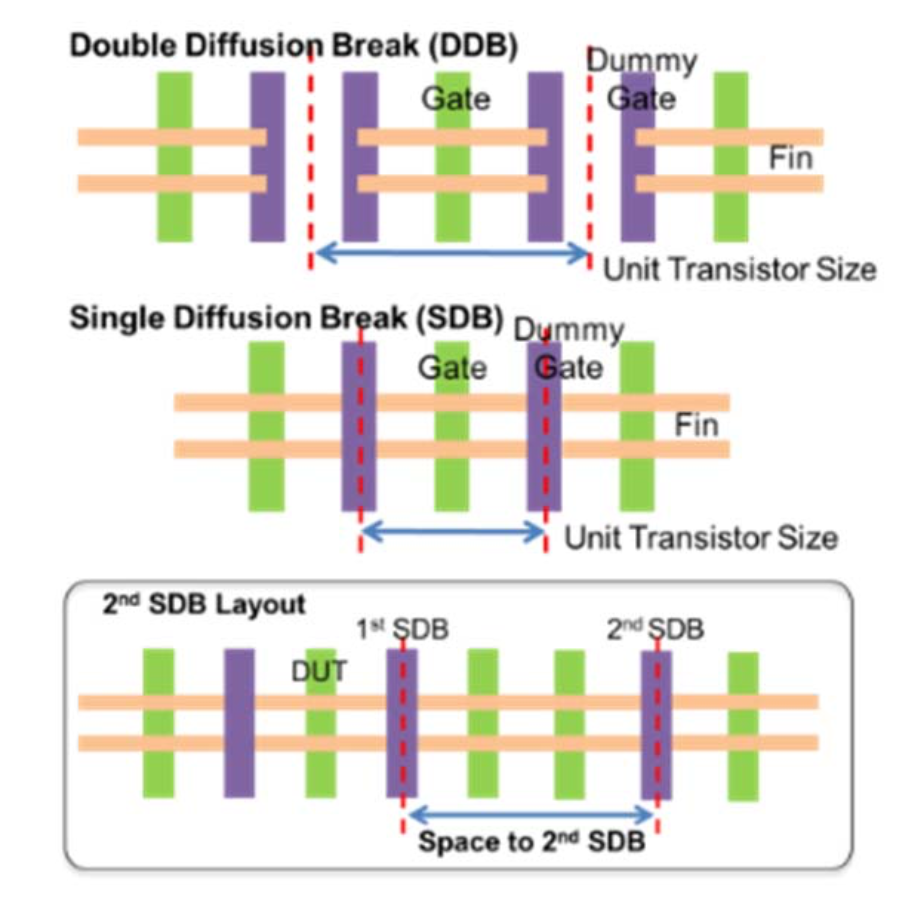
Image Single diffusion break reduces horizontal cell width but spacing has a variation impact
Although contact and the densest metal layers are to be patterned using EUV, Samsung will use a variety of multipe-patterning techniques based on ArF lithography for other masks such as those used to define fins. Jeong said just moving from multiple patterning to EUV for the critical layers is not enough to ensure effective area scaling from 10nm. The company went through a cycle of design-technology co-optimization (DTCO) to find other methods for improving density. Among the results were the addition of two specialized layout constructs that were defined to avoid common connection techniques to standard cells causing design-rule violations.
One “special construct” made it possible to reduce the track height of standard cells by one. “It improves scaling by 10 per cent and reduces power by 20 per cent,” Jeong claimed.
Another, L-shaped special construct allowed the removal of a dummy polysilicon contact and so make the standard cell narrower. “Special constructs give more design flexibility and achieve higher gate density,” Jeong said.
For the 7nm process, Samsung tuned the single diffusion break (SDB) that the company had used on the previous 10nm process. The SDB was introduced to reduce the wasted die area needed for diffusion breaks by merging two dummy gates on the outside of the abutted cells into one. The issue was that the SDB introduced a local layout effect that was a function of the spacing relative to a second SDB. “Tensile stress becomes more compressive,” Jeong said. “The more compressive strain makes PMOS Vt decrease and NMOS Vt increase. This kind of stress-related local layout impact could make the device variation higher.”
By performing some strain engineering to compensate for the effect, Jeong said the process designers were able to avoid the variation problems.