Chipletz pushes packaging design for AI, HPC and immersive use-cases
Austin-based start-up Chipletz has completed its first design of a Smart Substrate that aims to help deliver the increasing performance needed for artificial intelligence (AI), high-performance computing (HPC) and immersive applications such as those envisaged for the metaverse.
“As a fabless substrate vendor and chiplet integrator, we develop an advanced packaging technology that bridges the gap between the slowing of Moore’s Law and the rising demand for compute performance,” said CEO Bryan Black.
Black leads a team made up of AMD veterans and other leading silicon players. Its approach targets the creation of systems-in-package that allows for the integration of almost any die from any supplier.
The Smart Substrate aims to enable integration of almost any die from any supplier (Chipletz)
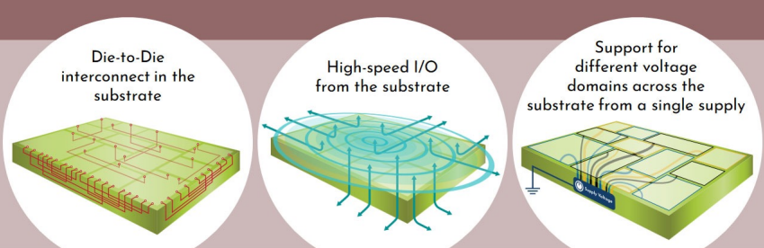
The Smart Substrate based platform therefore provides die-to-die interconnect and high speed I/O, and
supports different voltage domains from a single supply.
In evaluating its packaging tool options, Chipletz ranked them for the target of a very large SoC flanked by four high-bandwidth memory (HBM) stacks where the decoupling capacitors could be integrated into the Smart Substrate. The device measured 50x 65mm and had more than 8,000 nets connecting the dies using around 1.2 million vias with over 180,000 total device pins on a BGA containing 2,800 balls.
By using the Smart Substrate technology, Chipletz wanted to realize a packaging design with more than 150 reuse circuits. This reduced the number of metal layers to nine, against a previous version on a silicon interposer that needed 16 layers.
The work led Chipletz to settle on the Siemens EDA Xpedition packaging suite as it met seven core criteria required for the work.
- Support for high bandwidth memory HBM channel design
- Interactive performance on a very large design with very large connectivity structures
- Advanced substrate degassing capabilities
- The creation of complex power and ground structures using reuse
- Design tool and design flow automation and customization
- The ability to develop custom Smart Substrate-specific design rule checks
- Supplier domain expertise and technical resource availability and credibility
The work chiefly deployed three main parts of the Xpedition and PCB families from Siemens.
“We selected Siemens as they demonstrated their technologies’ capability and capacity, along with their expertise in advanced heterogeneous semiconductor package design,” said Black.
Chipletz has now completed its first design and now wants to make further packaging improvements with a focus on thermal issues, including thermal-induced mechanical stress. Here too, it is likely to work with Siemens EDA.