ETRI builds flow for AI chiplets
The Electronics and Telecommunications Research Institute (ETRI) is one of South Korea’s leading public research centers and it is now working on advances in AI processing by using a chiplet architecture.
For one of its latest innovations, the ABS1 Neural Processing Unit (NPU), it partnered with packaging giant Amkor Technology and vendor Siemens EDA to exploit some of the key advantages of chiplets over traditional monolithic designs: leveraging the latest 3DIC technologies, increasing performance and bandwidth while reducing power and cost.
The ABS1 NPU is implemented as a chiplet within a wider system and offers one quadrillion FLOPS (petaFLOPS) per second, equivalent to 10,000 standard applications processors within a single AI processor.
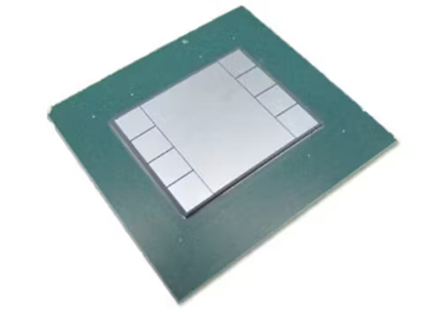
Figure 1. The ABS1 is the first petaflops AI processor with very high energy efficiency (Amkor Technology)
The wider system principally combines two of the NPUs with eight HBM memory stacks, with ten of these die integrated on an Amkor large-scale redistribution-layer interposer. Through Amkor’s relationship with Siemens Digital Industries Software, tools use to develop the entire system were Xpedition Package Designer (xPD), Xpedition Substrate Integrator (xSI) and Calibre 3DSTACK.
XPD provided functionality for interposer design with its physical reuse circuit feature and GDS direct-export capability. XSI assisted in delivering the best bump connections with 3DSTACK offering verification on the high-density design.
A full description of the flow that ETRI developed can be found here, and the institute plans to re-use this approach on further chiplet projects.
“The Siemens’ initiative to provide a CAD design environment for interposer and package substrate for advanced packaging has laid a foundational work for architecture designer,” said Youngsu Kwon, principal researcher at ETRI’s AI SoC Research Division. “At ETRI, we trust Siemens to further improve their xSI environment to better fit the design criteria of chiplets, which we consider to be the next-generation semiconductor architecture.”