Dense packaging focus for ECTC
This year’s Electronic Components and Technology Conference (ECTC), held in Denver at the end of May, will continue its focus on the role of packaging in keeping silicon scaling on track.
Though much of the R&D in packaging has concentrated on the needs of high-end computing and AI, with large-scale 3D integration schemes such as hybrid-memory cubes, one paper from IBM operates at the other end of the scale. The process developed at the computer company provides a mechanism for building complete systems on a substrate that fits into an area of less than 1mm2. The system described at ECTC includes a 32bit processor, memory, analog I/O with built-in temperature and chemical sensors, and an energy-harvesting power source. To integrate the sensors and other non-CMOS elements, the uses wafer-to-wafer (W2W) transfer.
To demonstrate the process, the researchers built heterogeneous chips thinned to 50-100μm, with lateral dimensions of several hundred microns, separated by ~20μm gaps, and with 10-20μm-diameter copper pillars. They say the process enables reliable and high-throughput system-on-a-carrier packaging with a diverse set of CMOS, GaN and GaAs chip technologies.
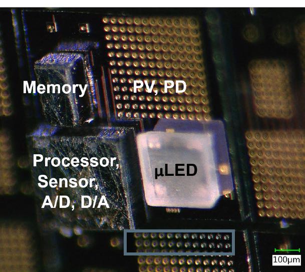
Image IBM's 1mm-square heterogeneous computer module
To demonstrate 3D packaging for high-end AI systems, a joint research team from KAIST-ETRI-AMKOR built a test vehicle for what they describe as a hyperscale-processor unit (HPU). This consists of a pair of neural processor unit (NPU) chiplets and eight High-Bandwidth Memory 3 (HBM3) chiplets. The team integrate all 10 chiplets onto a large-scale interposer with redistribution layers carried by a package substrate. High-density interconnect was used between the NPU and HBM to enable near terabyte-per-second inter-chiplet bandwidth.
To support denser logic and mixed-signal integration, Sony researchers will show how a successful electrical connection through three layers can be achieved, paving the way toward a process for three-layer stacked 3D heterogeneous integration. They will describe a chip-on-wafer-on-wafer (CoWoW) process, that uses a combination of face-to-back (F2B), chip-on-wafer (CoW), and face-to-face (F2F) stacking with 6µm-pitch copper-to-copper connections between the layers.
Bowing of the top chip was controlled to achieve void-free CoW bonding, and CoW bonding strength was simulated using elastic strain energy testing. The Sony researchers claim connections using CoWoW exhibited high reliability in stress-induced voiding and electromigration tests.
Teams are also looking more closely at the cost and yield of 2.5D and 3D integration. At ECTC, Intel researchers will describe an infrared laser debond technology that uses inorganic thin films to control laser release from silicon and other carrier wafers. They have performed transfers of back-end metal layers, 3-µm pitch hybrid-bond interconnects, and singulated chiplets from silicon carrier wafers to silicon receiver wafers without damage to any transferred layers, chiplets, or the silicon carrier.
They have also carried out damage-free infrared-laser debond of an organic interposer with two redistribution layers with up to 333 lines/mm on a silicon carrier wafer.
For lower-cost, high-volume systems that still need fine-pitch redistribution layer, Resonac has examined new resists to help build these interconnects on larger scale panels. Equipment limitations and potential warpage make it challenging to fabricate panel-format redistribution layers because of the need to apply photoresist material across a large panel with good thickness uniformity. Dry films are easier to use but have lower resolution traditionally compared to liquid resists.
The Resonac team will describe a new negative-tone dry film resist with a 1μm resolution and an aspect ratio of 6 on wafers and 1.5 μm resolution and an aspect ratio on a commonly used insulating build-up film, delivering a 3µm pitch on the lower-cost panel substrates.
Other sessions will examine reliability of large-scale 3D packages, integration for silicon photonics as well as work in emerging technologies such as quantum computing.