Heterogeneous integration calls for new approaches
Heterogeneous integration has the potential to overcome the yield and cost challenges presented by the growing headwinds associated with process scaling. But it may take a dramatic rethink of the ways in which SoCs are designed and assembled to realize the benefits.
In his description at VLSI Symposia of the decisions that his employer has made in its pursuit of multichip integration with both complete SoCs and chiplets, AMD corporate fellow Samuel Naffziger talked about the routing challenges that arise. For example, although using silicon as an interposer has advantages over redistribution layer (RDL) connections implemented in an organic substrate, it faces problems if the final system-in-package (SiP) needs to support high-speed, low-latency communications over its full surface.
FPGA makers such as Intel’s programmable systems group (formerly Altera) have for a number of years used silicon bridges to let them make serdes and I/O interfaces on an older or more specialized process that can then be coupled to primarily digital silicon fabbed on a leading-edge process. But these bridges need only support short connections. A purely passive interposer cannot easily handle traces of much more than a centimeter. Monolithic SoCs rely on the use of buffers and repeaters that are not available with passive substrates. Even if manufacturers can go to active interposers, the need for signal manipulation leads to distance-dependent latency, which in turn affects the performance of multithreaded software unless the threads are locked to specific cores.
The issues of non-uniform memory access (NUMA) led AMD to develop an in-package network based on a ring topology that could both normalize core-to-core delays and deal with the signal-integrity issues of running through organic-package RDL. That translated into protocols and serial interconnect choices that would provide the necessary support for deterministic latency and routing length.
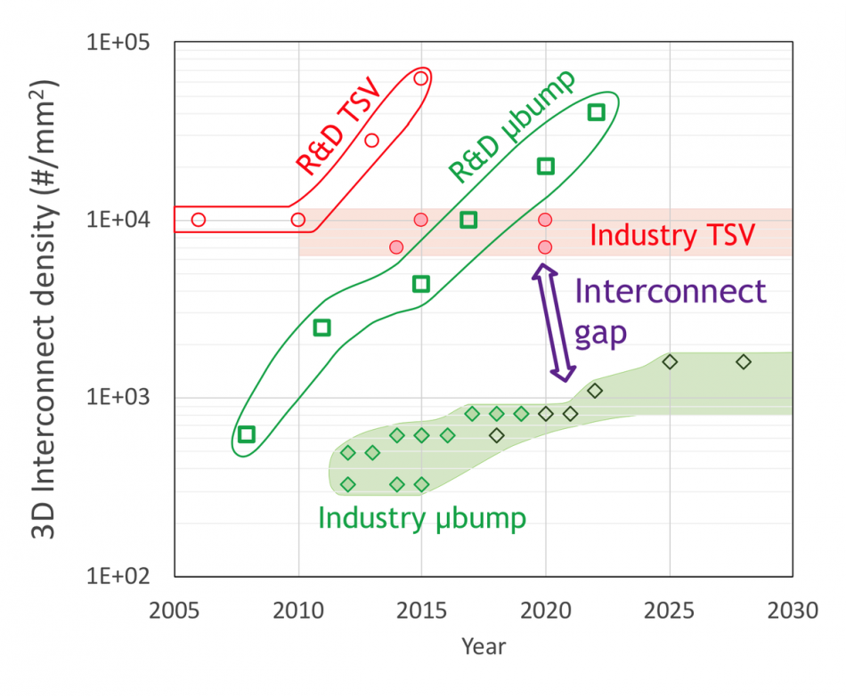
Image Projection of TSV and micro bump density (Source: Imec)
As part of his contribution for the VLSI short-course on heterogeneous integration Eric Beyne, vice president of R&D at research institute Imec, said a move to 3D interconnect provides an opportunity to maximize bandwidth. “The main 3D systems-integration driver is high-bandwidth logic-memory connection. Connections can be direct in the third dimension, reducing the interconnect length and with that, increasing the performance of the stack.”
But, as with in-package and 2.5D interposer-based integration, 3D stacking comes with its own set of difficult choices. Neither of the two main choices for forming the through-silicon via (TSV) connections are ideal. The via-middle and via-last approaches complicate back-end of line (BEOL) in different ways. “Generally speaking, via-middle gives you the highest quality,” Beyne said, but they call for larger keep-out zones to avoid adverse stress on nearby transistors, which reduces die utilization.
Mixing 2D and 3D connections comes with other complications. The pitch of TSVs can be much finer than the solder bumps normally used to form the connection between a die or a 3D stack to the package substrate. The problem with maintaining pitches on the order of 30µm, where they are today, is that it can make it extremely hard to make full use of bridge-type interposers to attach to I/O and then fan out from there. The interconnect you can fit into the bridge is limited by the perimeter dimensions of the chiplets – most of which will be designed deliberately to be core rather than pad-limited.
More bumps required
Beyne called for greater progress on microbumps or “bumpless” compression-based bonding that can bring connection pitch down to 2µm or even less. “A major challenge is that bumpless has no tolerance to particles. You need to make sure that the placement tools are very clean and, for current pick-and-place tools, this is not the case.”
Using denser microbumps or high-density bumpless interconnect would make it easier for designers to implement wide parallel buses and take advantage of lower latency for point-to-point connections instead of having to deal with the inherent delays of serdes. But the serdes bring the ability to take traces over much longer distances in the package substrate itself.
Mukta Farooq, distinguished research staff member at IBM, said the interconnect tradeoffs mean that there currently is no ideal answer for some of the main applications for SiP: high-performance AI processors. She pointed also to the problem of testability. Although yield for smaller chiplets will be better than large monolithic chips, especially if the chiplets can use the most appropriate process node for the circuitry they carry, assembly yield is a major potential weakness of the SiP approach.
Multichip modules have always been associated with the concept of known good die (KGD): devices that will pass tests when probed as bare die and so can be considered suitable for assembly. But while easy to say, it is tough to achieve in practice. Wafer-level probe has severe limitations that make it near impossible to achieve the kind of test coverage that can be obtained after a device has been packaged. And probing will be even tougher with thousands of connections at single-digit micrometer pitches.
Test headaches
“If we don’t know that the die is functional before stacking them together, the prospect of needing to throw away the whole assembly is extremely expensive. We can’t afford to do that. We need the ability to test them, which will drive the need for a new test capability on [bare] silicon. That may mean quite a lot of chiplet-specific logic is needed to support these tests. We will need to get the overhead of that down,” Naffziger said.
The nature of this on-chip circuitry is not entirely clear. In a webinar organized by MEPTEC, the general consensus was that KGD may be unachievable. But users might settle for “known not-bad die” in the words of Robert Patti, president of SiP specialist NHanced Semiconductors. If a die fails basic wafer probe, it can be discarded. Others can move to to dicing, even though those later operations may kill or damage the device before it goes into a package where rework and repair is not feasible.
“You plan for failure and you use known not-bad die as the starting point. You have to be able to take a number of hits and still end up with a product that’s sellable. Cell repair and test is the key to being successful in this next generation of electronic systems,” Patti said.
As a result, redundancy will be critical to making chiplet integration. How much redundancy will be a learning experience. “You have to be more open to communications with your customers and even within your own organization compared to where it all used to be siloed,” said Michael Alfano, fellow in the advanced packaging and memory technologies group at AMD.
Lihong Cao, director of outsourced semiconductor assembly and test (OSAT) provider ASE Group, said: “Sometimes we have to do screening in a pre-risk run to see if we can deliver high yield.”
Understanding failures
If a trial run fails, the question then becomes one of understanding how to fix the problem and determine whether it is fixable using the current architecture. “If everything passes wafer-sort test but fails after assembly, the question is how to analyze that yield. It can take a year to resolve who will pay for the fix. The challenge between OSAT, foundry and OEM is how we work together to provide high quality and low cost.”
Alfano said: “Experience has taught us communication and extremely strong partnerships are crucial. You have to be able to say ‘we are going to provide you with information on these failing device. We think this is your problem, though you might not agree with us’.”
In an interview with TDF, Brady Benware, vice president and general manager of the Tessent group at Mentor, a Siemens Business, said heterogeneous integration provides a natural extension for the growing connection between production test and lifetime reliability analysis. The recent acquisition of onchip-instrumentation specialist UltraSoC, which is already working with PDF Solutions on yield analytics, will help drive that. “You maybe need a better understanding of what you are brining together. Making sure different die can operate well together is going to require data. The on-chip instrumentation to collect that data and drive the cycles of learning will be a critical part of the industry’s learning curve. There is much more learning that the industry has to do to ensure reliability and consistency between chiplets that are brought together.”
Design communication
The need for effective, managed communication will extend back into design, said Synopsys principal applications engineer Rajesh Gupta at VLSI. Designers at different levels will need to be able to work to clearly defined specifications and also deal with different levels of access. “If die designs are not available during package design, you will need a specification to define them so you can move forward. On the other hand, you might have die designs available but you have the opposite prob: too much information. You may need to do work to abstract the I/O. In other cases, the package designers may not be authorized to access die designs directly.”
Mechanisms such as memory error-checking and correction may have to be rethought because existing methods that focus on correction across a band of chips do not work well in an environment where the aim is to maximize redundancy. The ECC logic might need to be itself distributed to prevent a failure in that section from killing the entire package.
Designers will also need consider approaches to architecture that they have not had to face before. “Stacking presents huge thermal challenges,” Naffziger said. “We need to design with the third dimension in mind. And, ideally, mix hot and cool sections of the design. But we have to consider that maybe they are not always hot and not always cool: maybe they alternate. For that we would need runtime power management.”
The end result is that decomposition into chiplets is only the beginning. The final system architecture may look very different once it ceases to be one based on a monolithic approach.