A*Star lays out SiP applications choices at IEDM
The first 75 years of the transistor, celebrated by the International Electron Device Meeting (IEDM) in December last year, were very much a story of monolithic integration. The next 75 look to be about heterogenous integration that, unless something comes along that proves to be simpler and cheaper, will proceed along multiple directions.
In an invited paper, Surya Bhattacharya, director of system-in-package (SiP) at Singapore’s A*STAR Institute of Microelectronics (IME), provided a useful bestiary of the options for heterogeneous integration in what is still an increasingly complex and evolving field, outlining where they align with application needs.
“End markets today are driving application-specific power, performance, cost, and form factor optimization, which is exactly the reason why package level scaling is so, so critical. And it is wafer level heterogeneous integration that can help us achieve package level systems scaling,” he said. “With the disintegration of large SoC comes the need to reintegrate heterogeneous chiplets This requires shorter denser interconnects which is made possible economically by wafer-level heterogeneous integration. Second, the limited PCB real estate in future system demands that system integration needs to happen at the package level.
“With benefits such as chiplet reuse and better yields, wafer level heterogeneous integration has become industry’s choice for realizing advanced SiP.”
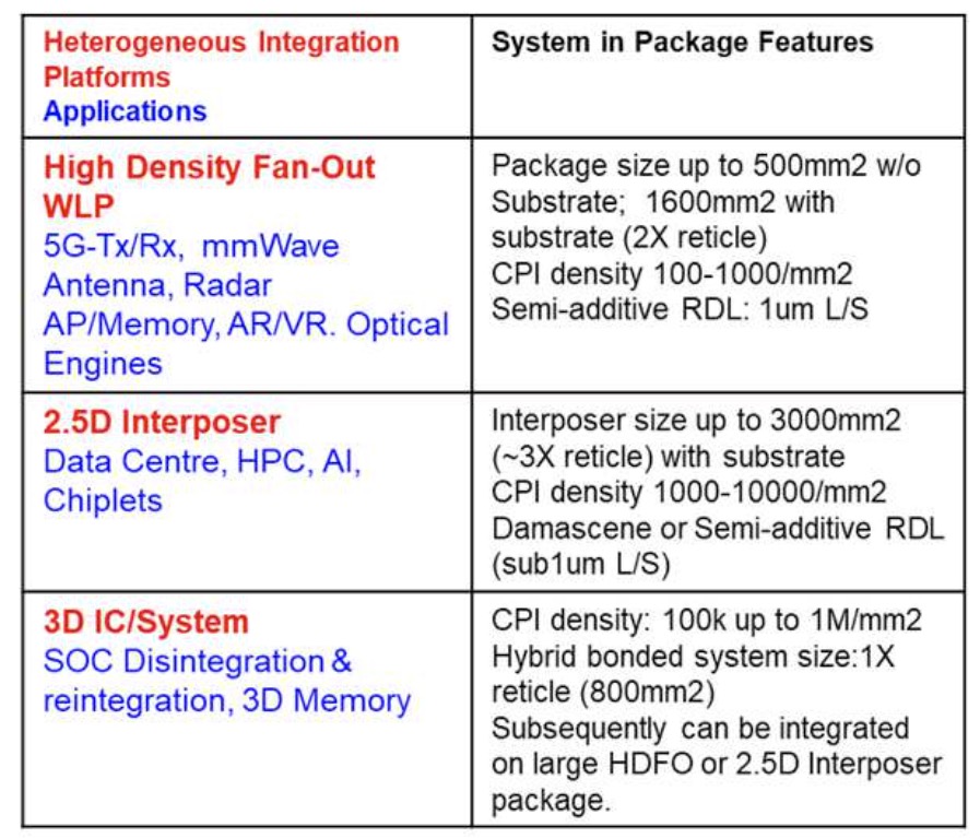
Image Applications and heterogeneous-packaging options
Bhattacharya outlined how data-center AI and high-performance computing designs are largely driving the markets for 2.5D interposer-based SiPs as well as 3DIC integration, thanks to their superior interconnect density and the ability to handle packages three times the regular reticle size to an area of 2500mm2, albeit with some drawbacks. “One of the challenges of silicon interposer is the cost of manufacturing,” Bhattacharya said.
Like Intel and its EMIB concept, A*Star has worked on a lower-cost compromise that uses silicon bridges that will handle traces up to 8mm in length, with multilevel redistribution-layer interconnect in an organic material to carry longer-distance traces.
For 3DIC, the institute has worked on reducing the cost of applying through-silicon vias with a “one step” process that etches the holes, applies a liner and deposits copper plugs once back-to-back wafers have been fusion bonded. According to Bhattacharya, this results in a 50 per cent saving in processing cost compared to existing wafer-to-wafer (W2W) stacking techniques. The other main development is on hybrid bonding to try to improve the inter-chip interconnect density.
For smaller packages, generally up to 20mm x 20mm, the institute has worked with both mold-first and RDL-first integration flows for SiP. The decision as to which largely depends on interconnect density the team has found. The mold-first has been used by the institute to make antenna-in-package devices for RF, extending that same technology to handle co-packaged optics for network switches. The RDL-first flow on the other hand was suited to both package-on-package and bare-chiplet designs in mobile computing, IoT, simpler AI devices with a large number of parallel traces between the chiplets.
Warpage continues to be an issue and Bhattacharya said they have found that traditional models do not take into account all the effects of the process flow. “We use [dynamic mechanical analysis] to obtain viscoelastic properties for dielectric materials and mold compounds and underfill materials. We also developed a novel technique to measure the cure induced shrinkage of polymer based materials by using [thermomechanical analysis],” he claimed. “For example, wafer-level warpage needs to be controlled for 12in processing. By using viscoelastic properties that we have extracted the we can accurately predict the warpage of fan out wafer level packaged wafers and this is very useful for us to enable process integration schemes.”
But overall, Bhattacharya sees this area as the future with upfront design needing to take into account how back-end integration will work. “System concept to system design and package design to prototype capability will hold the key to market success for heterogeneous integrated products of the future,” he concluded.