Scaling costs tip balance toward chiplets for AMD server processors
Although several of the sessions at the VLSI Symposia showed how CMOS scaling is continuing, the traditionally wise decision to opt for monolithic integration rather than multichip packaging is getting less clear. For AMD, the economics have come down strongly in favor of multichip integration for multicore server processors.
In a presentation for a short course on heterogeneous integration at VLSI, AMD corporate fellow Samuel Naffziger pointed out the steady rise in cost per square millimeter of silicon with each successive step down in geometry because of the increasing difficulty fab operators have in delivering the denser parts. They need more materials and the use of incredibly expensive lithography to stay on track.
Naffziger showed a graph that projected the trend in cost per square millimeter for a 250mm2 die, with a steady rise from 45nm to 14mm finFET, with that later node costing a little over twice as much on an areal basis as silicon made on 45nm. As that means five generations of scaling, cost per digital transistor dropped dramatically, so the small percentage rise each node was only noticeable in terms of analog circuit efficiency. However, since 14nm according to Naffziger’s figures, the price has risen dramatically: almost doubling in the transition to 7nm alone. Silicon area at the 5nm node is expected to cost five times as much as it does on 45nm and close to two-and-a-half times 14nm. Though this does not lead to the situation where transistors on later nodes are more expensive. Naffziger said this is a possibility in the future.
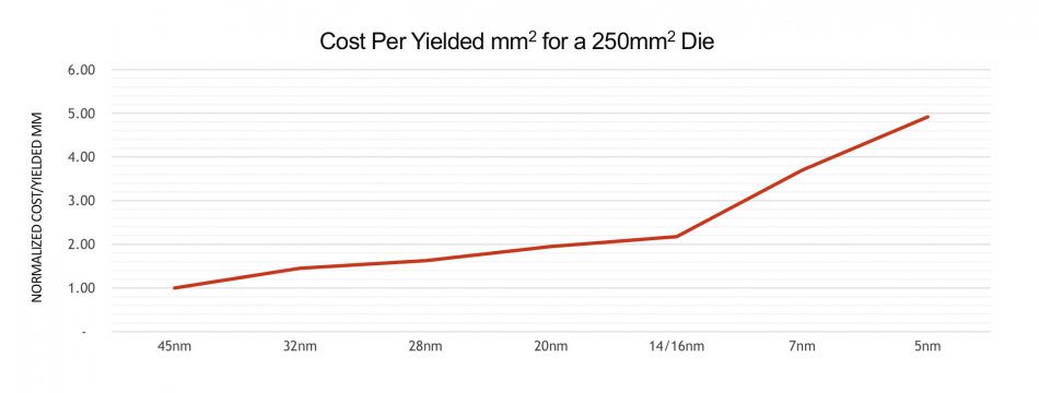
Image AMD's projection of silicon cost by area between nodes
“We need a different approach to things,” Naffziger said. He used AMD’s own experience with chiplets and multichip modules as a potential answer. For AMD, it has made migration to 7nm feasible, especially with the experience gained on processor-design projects that started three years ago.
“We started out with a 2017 server design that was technically an multichip module. Each processor could serve as a standalone eight-core processor. Combining them in one package enabled us to cost-effectively deploy 32 cores without breaking the bank,” Naffziger said.
The chief saving in moving to multichip processors was through yield improvements. “If you have a big monolithic 32-core design, you don’t get many of these on a wafer,” he explained, noting that such a multicore device would approach the lithography reticle limit. The yield improvements made possible by combining multiple chips on a substrate easily outweighed the cost increase of the more complex production flow and the redundancy of having to use multiple power-management devices.
Moving to a chiplet architecture potentially yields greater savings, which is the approach being taken for the 7nm generation. “A chiplet-based design is different to a multichip module. The die in a multichip module can be used standalone. Chiplets result from a decomposition of design and need other chiplets to function,” Naffziger explained.
From MCM to chiplet integration
One major avenue for cost saving that works with the increased silicon-area costs of highly scaled nodes is by decomposing functions into different chiplets. Naffziger said the processor core circuitry on the existing Epyc processors only consumed 56 per cent of the die area. The rest was what competitor Intel often refers to as “uncore”: the memory and I/O controllers. “7nm doesn’t provide a lot of benefit for analog and mixed-signal circuitry. If we are going to pay so much for 7nm, we want to make the most of the benefits,” he said.
Memory and I/O control was split out to the “IODie”, made on a 14nm process. “We ended up with what we call a CPU-compute die, which is a lot smaller than an original Ryzen chip and is 86 per cent CPU,” Naffziger noted. The other 14 per cent is power-management circuitry and serdes for the in-package communications fabric.
Naffziger pointed out the transition to chiplets and multichip packages is not necessarily straightforward. Trying to find a balance between routing density, electrical performance with today’s collection of packaging choices can be difficult when you have a multicore processor. FPGAs have largely adopted chiplet-based architectures just for I/O, which made the use of interposers and silicon bridges relatively simple. AMD needed to deploy a cross-package fabric but hit the problem that signal range in an interposer is limited without active repeaters. In the end, it made more sense to use an organic substrate with RDL routing but this would lead to extremely high routing utilization, which called for careful layout choices. The high resistance of RDL traces would also limit power delivery to the devices inside the package. This led to a redesign of the power-delivery network so that processors could take better advantage of local low-dropout regulators.
Performance scaling
The design changes did not just made it possible to get to high core counts. “The other thing we were after was the ability to configure these designs to cover the breadth of the server market. A bigger competitor would design individual SoCs to cover each corner of the market. But the use of chiplets has allowed us to depopulate the chips in a package and get cost-performance scalability,” Naffziger said.
AMD’s calculations indicated that a monolithic 64-core processor was unachievable, but entirely feasible using chiplets. A 48-core monolithic made on 7nm would cost twice as much as one based on a mix of 7nm core and 14nm I/O chiplets. Even at 16 cores, the chiplet-based design still worked out on the order of 60 per cent that of the monolithic option.
“This has set the stage for where we want to go. The market is becoming very diverse and dedicated accelerators can be much higher performance for an applications than a general-purpose CPU. We want to mix and match chiplets from other sources with our compute capability. Ideally, we would source some of those from third parties. It’s compelling but it presents a lot of challenges.”