Alternative scaling approaches form VLSI 2021 technology highlights
The VLSI Symposia on VLSI Technology & Circuits committee has published the program for its upcoming online event in June with the technology section providing an insight into the methods chipmakers will use for density improvements as conventional linear scaling becomes increasingly troublesome.
Imec researchers will describe work on one of the team’s ”scaling boosters”: the merging of the n- and p-channel transistors of a complementary pair into a structure the research institute calls a forksheet. This adapts the steps used to create nanosheet transistors, similar to those that Samsung will introduce in 2022 with its 3nm process, to form the complementary pair on either side of a silicon-nitride isolation wall. The approach represents a major reduction in the separation between the two transistors, which conventionally are formed as separate entities. In this work, the two transistors are less than one gate length apart at 17nm.
Although the forksheet is good for scaling, it represents a return to a trigate structure at the gate cannot wrap fully around the channel as one side of each nanosheet rests against the SiN wall. This reduces the effective channel control compared to the full gate-all-around (GAA) nanosheet structure.
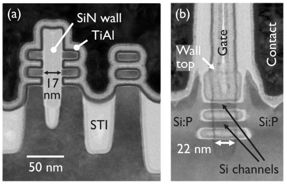
Image Cross-sections of the Imec forksheet and nanosheet structures
Short channel control in forksheets, according to the Imec team, is as good as independent nanosheet-based transistors, down to a channel length of 22nm. This is longer than the expected minimum gate length for sub-3nm processes, based on IRDS projections. The latest work, however, shows a way to implement both forksheet and nanosheet transistors in the same process, providing designers with the option to combine them to take advantage of the scaling and performance properties of either.
According to Imec, work on the cleaning steps after etching away sacrificial material in the forksheet stacks, has improved the on- and off-current behavior of the structure. The researchers attribute that to a reduction in interface traps that can form when the gate materials are filled in around the sheets. The gate deposition process allows the use of materials with different work functions for the n- and p-channel transistors.
Backside power
Another scaling improvement is likely to come from burying the power rails under the silicon surface. This will free up much needed signal-routing capacity in the metal interconnect as well as providing a further opportunity to reduce the overall track height of high-density standard-cell libraries. Another Imec paper will take that one step further with the use of extreme wafer thinning to make it possible to connect those rails to the power supply from the back side of the die rather than the front.
To demonstrate the possibilities, the team experimented with several thicknesses of silicon under the active layer from around 370nm to as little of 20nm with tungsten vias used to implement the power connection after bonding to a carrier wafer.
Working on a donor wafer that has finFETs with a fin pitch of 45nm and gate length of more than 20nm, the researchers tuned annealing steps after bonding to find enhanced NMOS mobility but a slightly reduced PMOS drive current.
Focusing on post-silicon transistors that may appear around the end of the decade, Intel reported on its work with the 2D-channel materials of tungsten diselenide (WSe2) and molybdenum disulfide (MoS2), for p-channel and n-channel transistors, respectively. One of the roadblocks currently preventing the rollout of 2D-channel materials is obtaining low contact resistance between the materials themselves and the source and drain regions. In this work, Intel claims it use of an unnamed novel contact material for MoS2 has resulted in one of the lowest contact resistances reported so far at 0.4kΩ·μm. For the p-channel WSe2 material, Intel has used palladium as the contact metal. The p-channel devices that use CVD WSe2 show a subthreshold swing of 89mV/dec, which is the best reported for PMOS on grown films. But the on-current remains behind NMOS.
In the back-end of line (BEOL), metal interconnect and via resistance are continuing headaches for foundries, with ongoing work to reduce the resistance by focusing both on the core resistance and that of barrier layers needed to prevent copper leaching into the surrounding dielectric films. IBM Research has used combinations of cobalt and copper to reduce the core resistance in a dual-damascene process, together with selective deposition of a tantalum nitride (TaN) barrier to reduce overal via resistance. The team expect high-performance computing (HPC) applications will combine these materials with high aspect ratio power rails to provide the best performance.
Transistors implemented in BEOL layers may provide a boost to overall system density and power efficiency through integrated power converters, though the performance of what are mostly thin-film devices will likely remain behind that of those built on the base silicon wafer. The gap may be narrowing with novel structures. Researchers from Purdue University will report on work with indium oxide (In2O3) 3D transistors that can be conformally coated on fin-structures or used for planar devices using an atomic layer deposition (ALD) process.
Planar In2O3 transistors implemented this way showed a relatively high mobility of 113cm2/V⋅s and a record high maximum drain current of 2.5mA/μm, using a combination of channel thickness engineering and post-deposition annealing. The team built a zero-VGS-load inverter using the devices that could support a voltage gain up to 38V/V and a minimum supply voltage (Vdd) down to 0.5V.