Samsung moves further into 3D for denser flash
Samsung described at VLSI Symposia this week how the company aims to implement its double-stack flash memory technology to push the number of layers in these devices to more than a hundred. In doing so, the company has identified ways to scale down device dimensions for further capacity gains.
Jun Hyoung Kim, senior engineer at Samsung, said the problem for conventional vertical-string flash structures is they are reaching the limit of what etch and deposition technologies can cope with. “It was necessary to prepare an infrastructure that would allow a next-generation device,” he said.
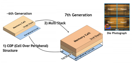
The increasing problems facing future flash memories were largely due to the high aspect ratios needed to construct the holes into which the stacks of flash transistors are formed. According to Kim, the complexity of trying to stay with a single stack for what Samsung regards as its seventh generation of flash technology is more than four times what it was for the fourth and double that of the technology’s predecessor. A move to a process that forms two stacks in series reduces this process difficulty to less than that of the sixth-generation technology and only about 40 per cent more difficult than the fourth.
“It is more effective to increase the number of stacked layers. The double-stack process drastically lowered defects in manufacturing,” Kim claimed.
Image Samsung's seventh-generation flash uses two forms of additional stacking
At the same time as switching to a double-stack process for the memory cells, Samsung has decided to make another transition into the third dimension by placing the memory array directly over the peripheral circuitry. Though this calls for more process steps to form interconnections, Samsung found the cost crossover for this cell-over-peripheral (COP) approach would take place between the sixth and seventh generations. The rearrangement of the peripheral circuitry, which reduced the distance to the cells, has improved read times by just over 10 per cent and programming times by 20 per cent.
Samsung took advantage of the move to the double-stack process and its lower aspect ratios to reduce the channel-hole pitch and improve bit density further. The result is an architecture that allows for a density of 8.5Gb/mm2 and a 70 per cent increase in capacity over the previous generation.
Although the aspect ratios in each stack are lower, Samsung made process tweaks to address problems such as stacks leaning over by tuning the stress imposed by the deposition of tungsten metal for the word lines and other process steps. The process team also changed aspects such as how source lines are connection to the memory cells and used a multi-step etch technique to improve the quality of the contacts made by the tungsten lines.
