VLSI Symposia delve into future process choices
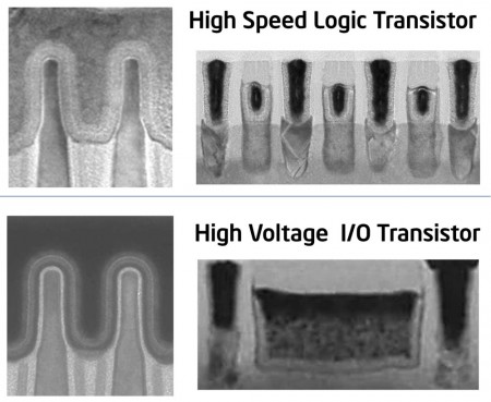
Among other presentations at the VLSI Symposia in Kyoto, Japan next month (June 15-18), Intel will describe its approach to a 14nm finFET process tuned for SoC use that keeps the metal and gate pitch of the processor version but employs a denser SRAM cell.
The HDC cell proposed by Intel covers an area of 0.0499µm2, coming down from the 0.0588µm2 previously reported. The SoC finFET process will deploy high-voltage transistors able to support voltages up to 3.3V for I/O and will include analog and RF features.
Looking further into the future, Intel will describe the use of gallium nitride for low-power SoCs rather than in high-power transistors and RF amplifiers where the material is used today. The company has developed a 90nm enhancement-mode MOS-HEMT hybrid – in contrast to the mostly depletion-mode devices currently encountered in high-energy applications – that could be applied to on-chip voltage regulators and RF circuits and open up more possibilities for local power conversion.
Image Cross-sections of the Intel 14nm logic and I/O finFET transistors
The transistors exhibit 3.6x lower on-resistance than silicon transistors intended for voltage regulators at an equivalent breakdown voltage. For RF, Intel claims the transistor structure offers higher RF power output at matched power-added efficiency than existing GaAs RF amplifiers.
For attempts to merge III-V materials with conventional logic, IBM and EMPA will describe work to bring indium gallium arsenide (InGaAs) into large-wafer CMOS processes suitable for high-volume production. The technique, which places the active InGaAs devices on insulator has been used to build gate-first, self-aligned finFETs with a 100nm-long gate and 50nm-wide fins.
Even further forward, a group from MIT, IMEC and KU Leuven will present results of experimental 15nm devices made from a combination of molybdenum disulphide (MoS2) and graphene, with the latter used as source and drain contacts. After building monolayer and four-layer devices, the researchers found the better results with the four-layer design, obtaining an on-off current ratio of more than 106 and a minimum subthreshold swing of 90mV/dec. A longer gate length brought the swing down to 66mV/dec, the best reported so far for MoS2 devices.
