Image sensors shrink at IEDM
This year’s International Electron Device Meeting (IEDM), taking place in mid-December, features a number of papers that seek to push the performance of image sensors, with two groups finding ways to overcome the inherent problem of trying to boost resolution without increasing silicon area at the same time.
Imec researchers, working with colleagues at the universities of Leuven and Ghent, have mimicked some of the attributes of the human eye with their proposal. They used standard backend processing on 300mm to create an array of tall silicon nitride waveguides in a silicon dioxide matrix. This structure acts as a wavesplitter array that segments incoming light based on wavelength in a manner analogous to the way the human eye segregates color detection by cell in the retina. However, the physical operation is quite different.
In the Imec construction, each waveguide splits a different frequency of light into symmetric and asymmetric modes. These propagate through the waveguide differently, leading to a unique “beating” pattern between the two modes for a given frequency. The beating pattern represent a certain color. The researchers said this technique enables further scaling of high-resolution imagers.
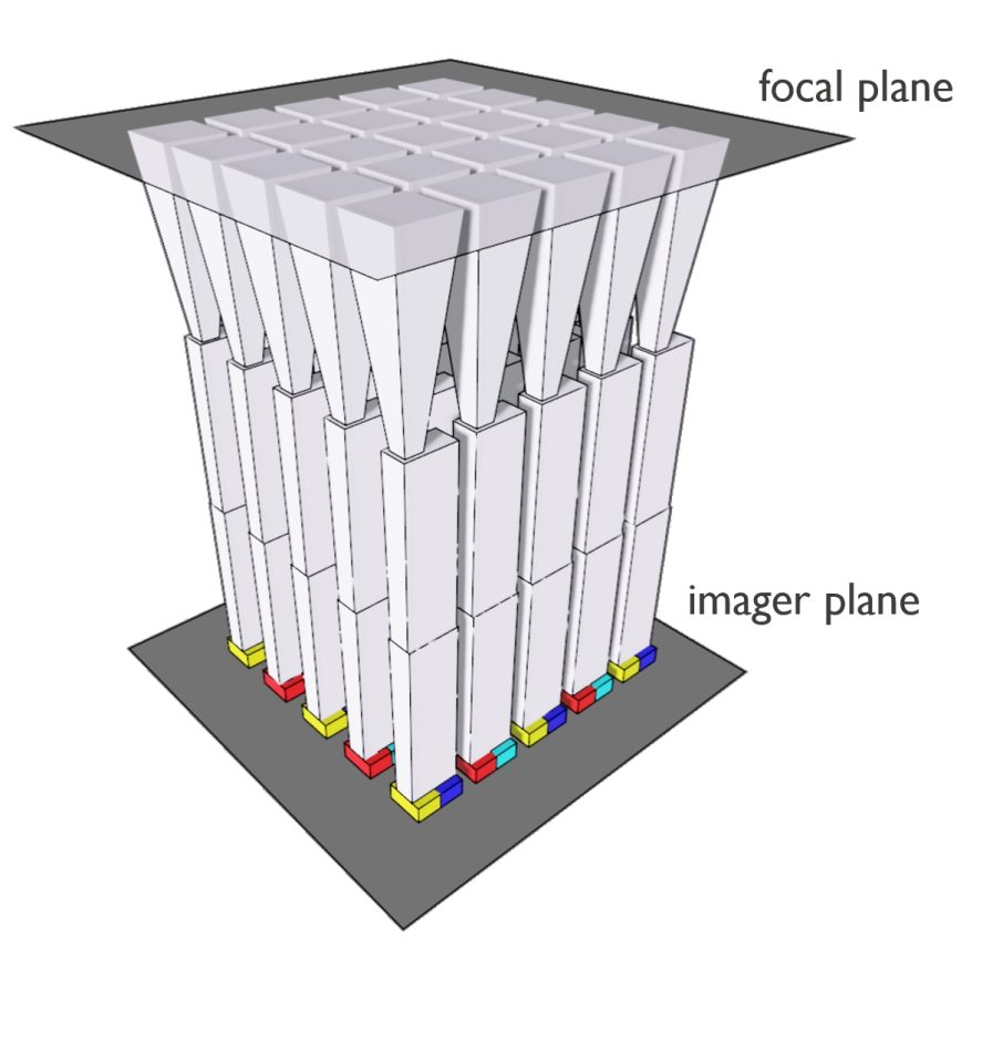
Image Imec's silicon nitride waveguide array structure
A Samsung team has focused on the decreased signal-to-noise ratio that comes with smaller pixels. Random telegraph signals (RTS) and parasitic capacitances are particularly troublesome. In their demonstration of a stacked three-layer 64-megapixel CMOS sensor architecture with 0.5µm pixels, the smallest ever reported they claim, a key feature is the use of copper-to-copper bonding to interconnect the layers. This reduces overall size as well as parasitic capacitance. The pixels demonstrated an 85% reduction in RTS noise and a 67% higher gain in light conversion efficiency compared to earlier work.
In their work on a three-layer image sensor, a Macronix-led team combined two novel device types with 20nm silicon FinFETs. The design includes DRAM-like devices based on indium-gallium zinc oxide channels coupled with phototransistors that use molybdenum disulphide that delivers a responsively of >1A/mW. Built on a 200mm silicon wafer, the architecture delivers logic, data retention of more than 1000 seconds as well as low-power working memory for computing-in-memory functions to operate on images detected by a 5×5 array of MoS2 phototransistors. Using fine-pitch vertical interconnects, the team claimed the approach will enable small form-factor and ultra-thin smart image-sensing systems.