IEDM 2020 highlights transistor and interconnect advances
At the upcoming International Electron Device Meeting (IEDM), a team from Intel will demonstrate one of the ways in which density improvements can continue as 2D scaling becomes ever more troublesome.
The approach echoes work by Imec on its CFET architecture, which appeared at the VLSI Symposia in 2018. With the CFET, which was proposed for the 3nm node, p-channel and n-channel transistors are stacked on top of each other to reduce the footprint of a CMOS pair. For this work Intel has used nanoribbons to achieve a similar space-saving arrangement using self-aligned processes. The combination transistor uses epitaxy to build a vertically stacked source-drain structure with the threshold voltage tuned individually for the two types of ribbon. A dual-metal gate completes the transistor to deliver a subthreshold slope of less than 75mV/decade and a drain-induced barrier lowering figure of less than 30mV/V for gates over 30nm long. Though the gates in this work are comparatively large, the Intel team expects significant cell-size reductions being possible through the self-aligned stacking.
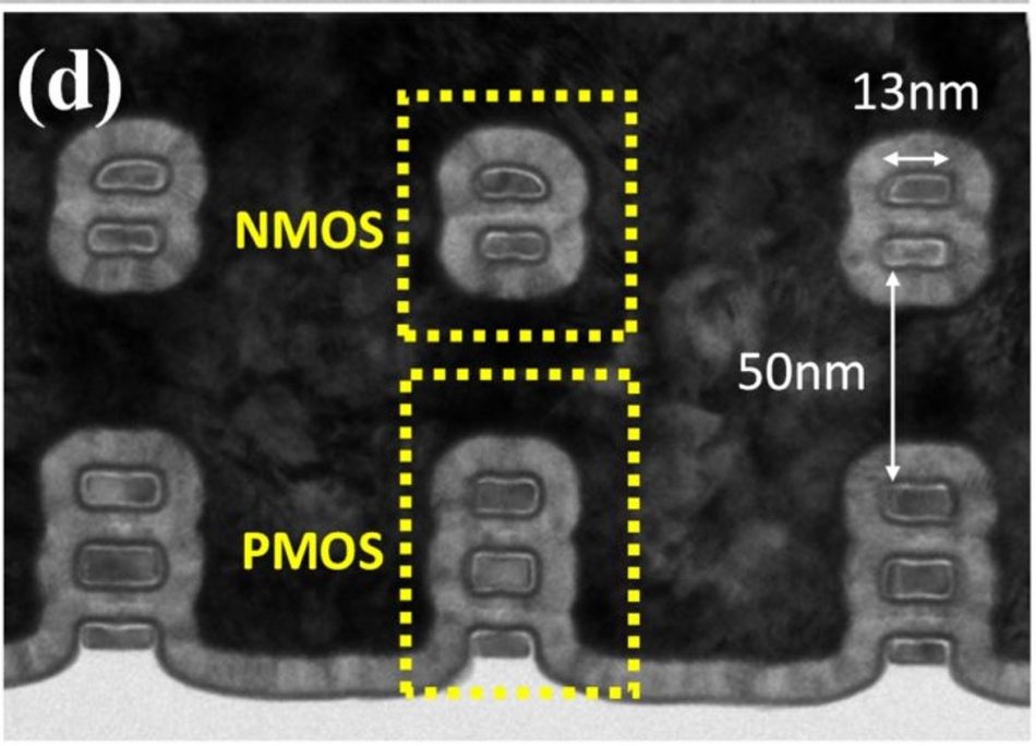
Image Cross-section of Intel's stacked nanoribbon transistor
Although transistor scaling is still a productive path, interconnect parasitics present a continuing problem for nanometer processes. A team at the University of California at Santa Barbara claims to have found a way to make one promising, low-resistance candidate work better with CMOS process. The compatibility has been a long-standing problem for graphene nanotubes and nanoribbons. The experiment builds multi-level graphene interconnects on top of a silicon dioxide and copper substrate that are compatible with existing back-end-of-line (BEOL) techniques though with edge-contact metal vias rather than top contacts. A scaling analysis performed by the researchers indicates that though there is an increase in via resistance, the use of graphene improves circuit performance by about 1.5x compared to a conventional dual-damascene process.
As graphene-like 2D materials are potential candidates for transistors that need to beyond silicon and III-V channels, Quentin Smets and colleagues at Imec have investigated how badly these devices might be affected by variability. The group looked at materials such as molybdenum disulphide (MoS2), which is one of the more promising candidate materials, and the impact of layer thickness and grain structure among other issues.
The Imec team simulated and built devices that could support a drive current of more than 100µA/µm and found that thinning the material provides the best results. Using a true 2D structure with just one layer of MoS2 versus three resulted in a strongly reduced subthreshold slope and threshold-voltage variability. Overall variability was comparable to silicon finFETs.
Taking place from December 12 to 18, this year’s IEDM is a virtual event that includes six focus sessions on issues facing semiconductor: device technologies for cryogenic electronics; advances in wide-bandgap semiconductors; future interconnects; technologies for 5G communications and beyond; energy harvesting; and the design-technology cooptimization of logic and memory.