Intel and ST stake claims to foundry low power designs
With both Intel and STMicroelectronics looking to offer foundry access to, respectively, their finFET (aka, in Intel’s case, tri-gate) and fully-depleted silicon on insulator (FDSOI) technologies, both took the chance at DATE to show how they are pushing the envelope for low power design.
Intel Labs described both a 32nm planar CMOS and a 22nm CMOS tri-gate SIMD accelerator capable of near-threshold voltage (NTV) operation, across a wide dynamic range.
Some of the increasingly familiar advantages of finFETs were very much to the fore, including the improved DIBL and steeper subthreshold swings that help designers realize low-voltage operation at reduced leakage.
However, presenter Vivek De, of the company’s Circuits Research Lab, offered a few more pointers as to the design goals that need to be set for NTV work, specifically those that address “failures at low voltages due to supply noises, temperature excursions, aging-induced degradations, as well as workload and activity changes”.
“In particular, [you need] techniques for dynamic adaptation to environmental variations, and error detection, preemption and response… Fine-grain power delivery and management are essential for maximizing the overall energy efficiency at NTV. Efficient voltage regulators, fast voltage control and low-overhead implementations of multiple voltage domains are a must for realizing the full potential of NTV designs,” he said.
A joint ST-CEA Leti presentation described an implementation of an ultra wide voltage range design on FDSOI with ultra thin body and buried oxide (UTBB).
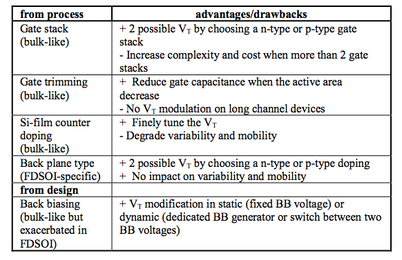
“The source and drain are raised to reduce the access resistances. There is no channel doping nor pocket implant, making the process as simple as bulk. The buried oxide (BOX) thickness is 25nm, leading to a good trade-off between drain/source-to-substrate parasitic capacitance and body factor. A backplane, either n-type or p-type, is implemented underneath the BOX to improve the short-channel effect and adjust threshold voltage. Back bias or hybrid/bulk technology is feasible after removing the BOX,” the research team said.
The thin BOX helps to add ‘knobs’ that allow a design to be tuned more in the sense of adaptive rather than dynamic voltage and frequency scaling. It creates a multiple threshold-voltage platform that can be adapted to the best trade-off between power and performance.
“[The BOX] creates a back-interface, which can be thought of as a back-gate, whose polarization value modifies the threshold voltage (Vt) of the transistors. The body factor, representing the Vt sensitivity to the back-gate voltage, is equal to 85mV/V for a 25nm BOX. Given that the back-gate voltage (back bias) can vary over a 2V amplitude, the Vt value can be greatly modified dynamically, enabling circuit designers to define several operating points,” ST and CEA-LETI explained.
“The second advantage of this thin BOX is that, combined with an n- or p-type backplane (a doped area beneath the BOX), it can bring transistors with two different Vt values, for the same gate stack. It means that the technology offers different ways to modulate the threshold voltage, first by providing a multi-Vt platform and secondly by enabling an efficient body biasing at circuit level.”
In essence, the adaptation can be largely tweaked by using forward or reverse back bias, respectively increasing or decreasing the Vt as fits the end application.
Threshold voltage ‘knobs’ for UTBB FDSOI designs (Source: ST/CEA-LETI)
The approach was benchmarked against test IP blocks, including an ARM Cortex A9, for its adaptability to 28nm fully-depleted (FD), low-power (LP) and general-purpose technologies.
For both companies, the presentations were largely about saying to potential customers: “We have this, and we can do it.” Certainly, both Intel and ST now have to do a lot more in defining what the foundries see as ‘technology leadership’. Intel is building its third-party manufacturing business and ST’s is now under more pressure following the dissolution of the ST-Ericsson joint venture, its flagship customer for FD-SOI.
STMicroelectronics used a lunchtime session on FDSOI at DATE to claim that it would be able to make devices on the process as cheaply as on bulk, by the end of the year. It also laid out a roadmap for its FDSOI process which sees the BOX layer being thinned as minimum lithographic dimensions are reduced, which improves the effectiveness of back-bias control over threshold voltage. Laurent Malier, director of CEA-Leti, said that back-bias control should be seen as a new systemic optimisation technique.