FinFETs face planar fightback at IEDM
The finFET may appear to be the device of choice for future process generations, mainly because that’s the choice that Intel has made, but it is not over yet for the planar transistor.
IBM has been developing planar devices on extremely thin silicon on insulator (ETSOI, also known as ultrathin body SOI or fully depleted SOI (Guide)) substrates for years, using the extremely shallow (>10nm) channel layer to achieve the kind of short-channel leakage control that the finFET (Guide) gets by raising the channel out of the substrate.
In a bid to improve the balance in performance between nFETs and pFETs on this substrate, a team led by IBM will discuss its work creating a pFET using a strained SiGe channel, and an nFET on a Si channel, at 22nm geometries. A paper abstract says that this hybrid approach was made possible using a process that put the shallow trench isolation in place last.
As is traditional, the paper uses the performance of a ring oscillator, with a delay of 11.2ps/stage at 0.7V, as proof of the value of the approach.
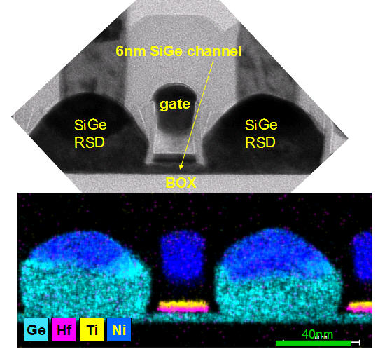
The image above shows, at top, an SEM cross section of the device, and below that an energy-dispersive X-ray spectroscopic view of a SiGe-channel pFET with a 6nm channel thickness, 22nm gate length, 100nm contacted gate pitch, high-k/metal gate architecture and in-situ boron-doped SiGe raised source/drain.
There will be more detail on IBM’s planar challenger to the growing finFET orthodoxy at December’s International Electron Devices Meeting in paper #18.1, “High-Performance, Extremely Thin SOI (ETSOI) Hybrid CMOS with Si Channel NFET and Strained SiGe Channel PFET,” by K. Cheng et al, IBM.