DATE: ARM proposes ‘unit of compute’ as basis for energy-efficient systems
ARM used a keynote at DATE this week to propose a basic ‘unit of compute’ that could be used to build more energy-efficient computation systems for applications ranging from mobile phones to high-performance computing (HPC) clusters.
John Goodacre, director of technology and systems in ARM’s CPU division, began by describing the evolution of multicore architectures at ARM. In its first phase, early in the last decade, an ARM multicore SoC design used a CPU, such as the ARM1176, coupled to a DSP, such as TI’s C64x family, in TI’s OMAP2 architecture. Communications between the two were handled using a mailbox-like strategy.
The second phase saw the introduction of the ARM MPCore, designed to make it easier for programmers and SoC integrators to work with multicore architectures. These one-to-four-core designs included an interrupt distributor, for high performance and low latency interprocessor communications, and a snoop control unit to ensure cache coherency among the on-chip cores.
Why take on the complexity of building a processor out of four cores, whose operations have to be carefully coordinated through a series of quite complex mechanisms? Goodacre said that the idea was to enable system architects to split a processor workload across several cores running at a lower clock rate than it would take for one core to handle the whole workload, leading to greater energy efficiency.
Energy proportionality
“A lot of people think multicore is a performance play, but for us it’s always been about that energy proportionality,” Goodacre said, adding that the approach had sold well to customers in markets such as digital still cameras.
These early multicore architectures also included interfaces which would later become critical to the ‘unit of compute’ concept – a generalised interrupt controller, an ‘accelerator coherence port’, and a master port that could separate data traffic out of a subsystem at the CPU level.
The third phase of the evolution of ARM’s multicore approach came with the introduction of the big.LITTLE architecture, which couples a high-performance core (anything from a single A8 core to a quad-core A15) to a lower-performance and more energy-efficient core, such as an A7. The idea is to match the performance, and hence energy consumption, of the core to the demands of the application code.
“We want the largest fidelity between the dynamic range of the performance demands [of the application] and the power consumption [of the cores],” said Goodacre. “big.LITTLE is all about maintaining that dynamic range by using multiple clusters of cores.”
He argued that this will be increasingly important as the semiconductor industry moves to finFET processes (Guide), which have flatter dynamic voltage/frequency scaling (DVFS) curves than planar processes. This limits a designer’s ability to match power consumption to processor load by adjusting the supply voltage and hence the clock frequency.
“As DVFS curves flatten, you need more of those curves to achieve the same dynamic range,” he said.
Unit of compute
Goodacre went on to define the ‘unit of compute’ concept as the “domain of the hardware and memory map that is owned by a single operating system.”
A ‘unit of compute’ has a computation engine and memory, a local coherent interconnection scheme, a port into that interconnect scheme which provides a coherent view of the memory hierarchy to the outside world, and ports out of it which provide a path to local memory, and a path to remote memory partitions.
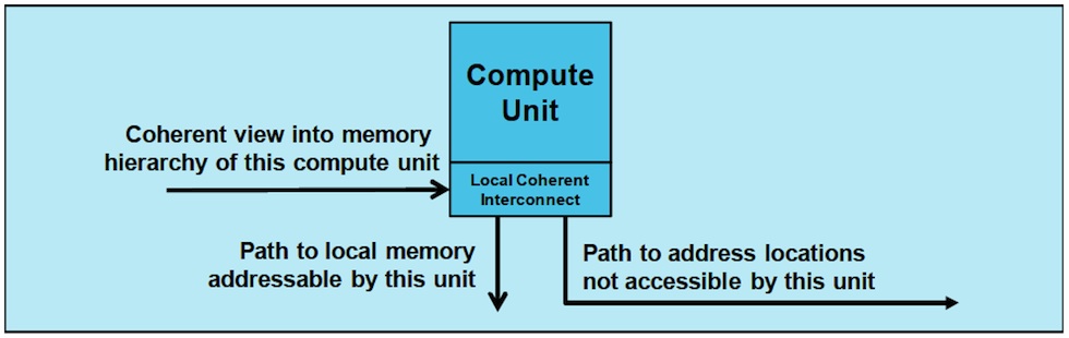
Figure 1The unit of compute concept (Source: ARM)
Hardware accelerators can be accommodated locally to a CPU within a ‘unit of compute’, or connected to whatever scheme is used to interconnect multiple units of compute.
ARM has already implemented some of the unit of compute concepts in its CoreLink CCI-400 cache-coherent interconnect scheme:
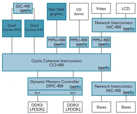
Figure 2 This interconnect scheme embodies 'unit of compute' concepts (Source: ARM)
and in its CoreLink CCN-504 cache coherent network scheme:
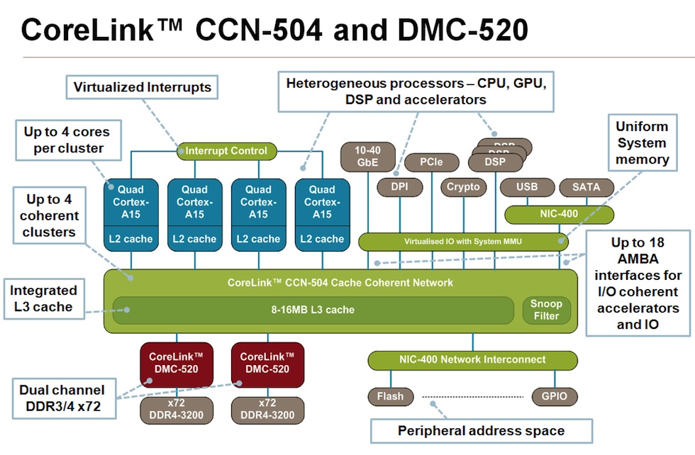
Figure 3 This cache coherent network could be used to interconnect 'units of compute' (Source: ARM)
Referring back to similar ports on ARM’s earliest multicore offerings, Goodacre said: “It turns out we have been building compute units for three product generations.”
Future architectures
“How can we use the concept of compute units to scale outwards?” Goodacre asked. “The move to 64bit allows us to have a large global address space, and the two types of interface allow us to join things together.”
The v8 architecture that introduces the 64bit address space also defines two coherence regions in its page table – an inner and an outer shared coherent region: “We’re not doing anything with that today, but it will be interesting to see what we could do with it in future.”
Goodacre sees a variety of options for interconnecting ‘units of compute’ in larger clusters, such as a shared memory approach taking advantage of the 64bit global address space of the v8 architecture, or a more network-like strategy, depending on what is appropriate for the target application.
A pair of ‘units of compute’ could be connected ‘back to back’, but linking millions of units would mean turning to strategies like those used in supercomputing, such as the message-passing approach of HPC clusters, or the directory-based coherence mechanisms of NUMA (non-uniform memory architecture) machines.
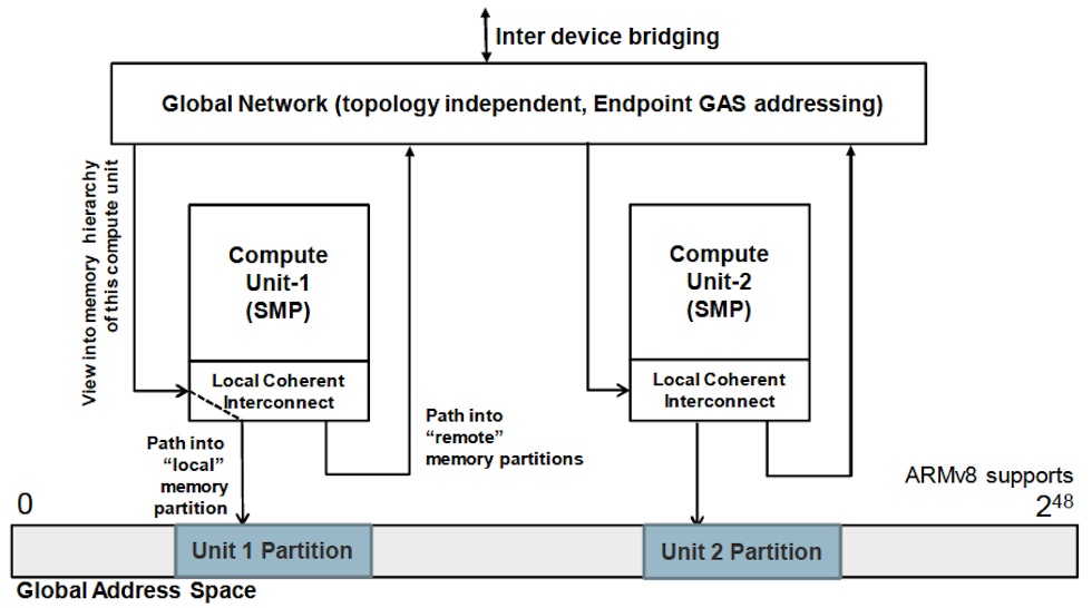
Figure 4 ARM's scalable global architecture builds on its unit of compute concept (Source: ARM)
ARM is already involved in two European Framework Program 7 projects that are developing building blocks for more energy-efficient computing – ENCORE, which aims to make it easier to exploit application parallelism, and Mont Blanc, an effort to build an energy-efficient, high-performance computing prototype. It is believed to be proposing a third Framework Program project, to produce a basic hardware building block for such an architecture, instantiating one or many ‘units of compute’ on the chip.