Sustainability work puts numbers on chipmaking production at IEDM
Shifting to low-carbon generation for electricity would do much to cut the carbon footprint of semiconductor processes according to work shown at this year’s International Electron Device Meeting, though the fabs would also need to work on capturing and recycling chemicals, particularly for future memory devices.
This year saw the conference focus on sustainability in manufacturing, creating a track that explored how much energy the processes use and their resulting greenhouse-gas emissions. The good news? Earlier predictions of the environmental impact pointed to higher emissions than those estimated in comprehensive analyses performed at Imec. The bad news? Resource usage is high and moving up as a natural consequence of the complexity of the processes involved.
Semiconductor production is hardly alone in the technology-intensive industries in what it adds to the embodied emissions of an end product. The overarching rule is: the purer the raw materials and processes need to be, the more energy they will consume. Semiconductor production has a few other issues, however. The important one is that some of the best chemicals for the job have an intense greenhouse gas effect, way beyond that of carbon dioxide. Fab operators have been aware of the issues of one particular etching agent for some years – sulphur hexafluoride – and have been seeking to cut down on its use. However, as it is very good at the job, the other direction has been to get better at capturing and recycling it.
Design implications
From a design perspective there is a tradeoff. In principle, digitalisation makes other processes more efficient and in areas such as motor control and green energy, more advanced semiconductors can more than pay their way once the lifecycle emissions are taken into account. On the other hand, the advantages of artificial intelligence are more difficult to assess against the huge embodied carbon total for the systems being installed now. Today, a large language model might need to run across 20 GPU blades that may wind up being retired after just a few years in service. More efficient AI systems can score two benefits: they use fewer accelerators and they may even be able to use accelerators built on slightly older and less carbon-intensive processes. Assuming this does become a factor in selection, which will depend on the use and level of carbon pricing globally, the key element is knowledge about how big that tradeoff is. It may be that scaling always outweighs the environmental change.
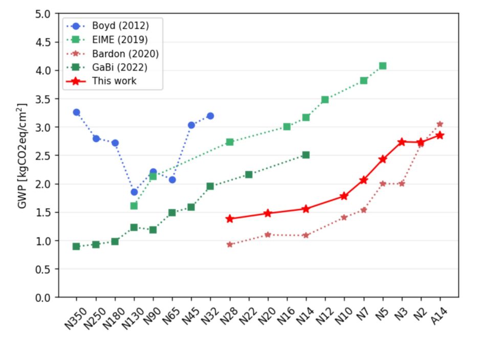
Image Graph of several recent carbon-footprint studies
Imec released some of its data publicly ahead of the conference in the form of an internet-accessible model, a body of data built up over the years in work for clients to estimate their energy and carbon budgets. At IEDM, Lizzie Boakes and colleagues presented a view of how embodied carbon emissions change from the N28 node to the future A14 generation. They used a 10x10mm die as the unit assessed at each node rather than scaling material and usage based on a constant transistor-and-memory count. So, the cost savings of scaling need to factored in to the estimates. As the electricity supply varies greatly from region to region, the study employed a weighted average of semiconductor production and matched that to the mix of fossil and low-carbon sources in each of the key regions to come up with an estimate of emissions based on energy. Additionally, they computed the sensitivity to electricity-generation emissions across the generations. They found that for a low-carbon energy source, the emissions of A14 would most likely not be much more than those of N28. At the current energy mix, 10sq mm of silicon at the A14 node emits almost twice as much as 10sq mm at N28
Compared to earlier work in this area, Imec’s team came up with figures that suggest some previous studies have overestimated emissions, though the overlap between those studies is partial. The total-emissions estimates from one study performed by Bureau Veritas with its EIME tool could be as much as double those of Imec’s for the N28 to N10 nodes, though the gap closed a little on the later nodes. The study also showed a small but tangible improvement in environmental performance that came with the introduction of EUV lithography at the N7 node.
Memory chemicals
Techinsights’ own work on a similar approach, presented by Scotten Jones also took in the environmental economics of memory devices, particularly 3D flash, which depends heavily on etching chemicals. The work found that up to around 130 layers, the increase in carbon emissions was negligible on a per-layer basis. Past 200 layers, the emissions begin to increase more rapidly though the numbers still favor scaling, if the assumptions hold for these far more ambitious structures. A 1024-layer stack would likely produce four times as much carbon equivalent emissions as a 128-layer chip, but should be able to deploy significantly more bits per square millimetre. The rate of increase in chemical usage is higher than for energy, though electricity consumption also more than doubles from a hundred layers to a thousand. Jones pointed out that transition from 2D DRAM to 3D DRAM will lead to a much greater increase in chemical increase. The analysis predicts carbon intensity will double in one step from the 0a generation to 3D DRAM.
Equipment suppliers are looking at how to help fab operators tune their processes. Benjamin Gross and colleagues from Applied Materials described the tools, which include Imec’s Netzero platform, the company is now using to assess the sustainability of the processes it supports in the fab. The work has translated in downstream tools, such as EcoTwin, which monitors chemical and energy use of fab equipment in real time. Applied sees the data being used to design new recipes that can demonstrate lower emissions and chemical use. Another output is the Sculpta software, which manipulates mask shapes to cut out some of the double-patterning steps that might otherwise be used on EUV equipment. Using Imec’s estimation software and database, Applied estimates the change can save around 15kWh of energy per wafer and its associated carbon emissions.