7nm process with EUV to feature at VLSI
Samsung Electronics will describe at the upcoming VLSI Symposia how its engineers have applied EUV to a number of layers in a 7nm finFET process.
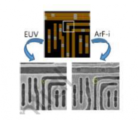
According to Samsung, single-pattern EUV is used for middle-of-line (MOL) and fine-geometry back-end-of-line (BEOL) interconnect between finFETs and supports a contacted poly pitch of 54nm. Fin pitch on the process is 27nm. The team claims the reductions in device size and other process changes compared with the preceding 10nm process supports up to 30 per cent fast switching and a power reduction of up to 60 per cent. Evaluation of the lithography showed an improvement of 70 per cent over immersion ArF exposures.
On test chips, the engineers have implemented an SRAM cell that measures 0.0262µm2 in densities up to 256Mb. To help get there, the designers used a single diffusion break to isolate devices in different active regions. The team says its process meets the requirements for negative-bias temperature instability (NBTI).
Image Comparison of EUV and immersion lithography fidelity on 7nm Samsung process
Samsung will join Qualcomm in describing the use of the 10nm finFET to support SoC manufacture. Optimizations made for the second-generation 10nm process led to a 40 per cent increase in processor performance, the team claims, and a 10 per cent increase in battery life. Half-node scaling to an 8nm process together with the use of quadruple-LE patterning provided a scaling improvement of 15 per cent, with gate pitch falling from 68nm to 64nm.
Among other threads that focus on memories and sensor technologies for the IoT, the VLSI Symposia taking place in Hawaii mid-June will include a number of papers that demonstrate advances in leading-edge processes. One of them from GlobalFoundries describes the use of nanosecond laser annealing to reduce the resistivity of copper BEOL interconnect by 30 per cent. The annealing process helps increase the average size of copper grains in the wires and, according to the team, does not harm mechanical stability.
Looking further ahead, research institute Imec will present progress on the manufacture of vertical-nanowire transistors based on germanium alloys. The team claims the initial results demonstrate performance similar to that of the best published germanium-based finFETs, with on-current of 500µA/µum and off-current of 100nA/µm.
