Panels see congestion and resistance dominate the leading-edge node battle
Placement-aware synthesis and an array of post-layout recovery steps have helped drive up the clock speed and silicon utilization of a series high-end SoCs on leading-edge processes developed by customers of Synopsys’ implementation tools.
In two events organized by Synopsys on Monday (19 June, 2017) at DAC, speakers from HiSilicon, Qualcomm, Renesas, and Samsung described how they used ICC II and other tools to handle the consequences of the introduction of DFM techniques for 10nm and now 7nm processes – with logic-level optimizations forming a key part of the toolbox.
“Each move to a new node comes with its own set of unique challenges. For example, we have seen a significant increase in the via resistance compared to prior nodes,” said Qiuling Zeng, senior ASIC designer at HiSilicon. “Collaboration with ecosystem partners is critical to our success.”
Rapid transitions
“In the last five to six years we have gone through six to seven nodes starting with variants of 28nm,” said Balaji Velikandanathan, quality engineer at Qualcomm, and the company is not expecting to slow down. “We are talking about [going from] inception to tapeout in nine months and a new process node every year.”
The use of 10nm technology by Qualcomm on the SnapDragon 835 mobile processor reduced die area by 35 per cent and power by a quarter, compared to its predecessor.
The aim of the migration to 7nm is to push frequency to 3GHz and beyond while keeping cell utilization above 70 per cent. “And reduce dynamic and leakage power by 30 per cent compared to the previous generation,” Velikandanathan added.
Although Qualcomm needs to maintain a high pace of development, the arrival of 7nm processes introduces additional problems for designers. The challenges, he said, are complex new design rules, increased resistance in the tight-geometry interconnect layers, and variation idiosyncracies in low-threshold transistors.
The big issue for low-threshold transistors in advanced processes is the way in which the variation has become non-Gaussian, with a fatter tail on the slow side. This makes timing estimation during placement and routing more difficult for the tools.
Via pillars
One consequence of the increase in metal and via resistance in the critical layers is the adoption of the via pillar, also known as the via ladder. Willy Chen, deputy director of the design and technology platform at TSMC, said designers working with the previous node were encouraged to use the technique of layer promotion, in which high-speed routes are pushed higher into the metal stack to take advantage of their lower resistance. The via pillar is intended to improve current delivery in the connections between logic gates and the interconnect that gets promoted.
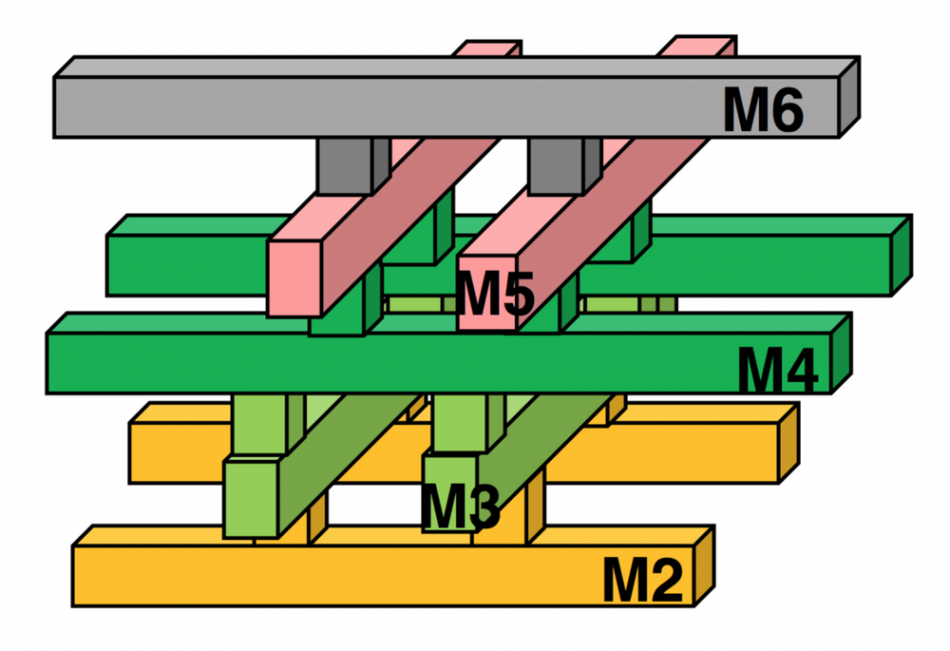
Image A typical via-pillar structure
A via pillar is a structured alternative to conventional redundant vias, introduced to deal with factors such as via resistance, the shape variability of double-patterned critical layers, and electromigration. The pillars use closely spaced pairs of vias that lie in the preferred routing direction for each layer, forming a lattice configuration with metal lines where the via needs to pass through several interconnect layers.
“The via pillar doesn’t come for free,” said Velikandanathan. “It uses additional routing resource and places additional challenges on the router.”
Chen noted: “There is an overall via area increase but it offers multiple routes for current and helps to reduce the path delay.”
The Synopsys tools perform via pillar insertion after placement, as they work on timing. Results from HiSilicon indicated that big improvements in performance are possible with a relatively modest use of via pillars and promoted-layer routing. Zeng said her team hit timing targets on the most recent completed project by using the fatter pillar structure for 10 per cent of its vias.
Power-saving banks
The issue of power consumption, particularly the relative increase in dynamic power that accompanied the introduction of finFET processes, is promoting the use of techniques such as threshold voltage optimization and multibit register banking.
“Using 4bit [registers], for example, reduces dynamic power,” said Joe Walston, senior staff applications consultant at Synopsys. “Vt selection: that also starts early in the design flow, because Vt selection is so important to be able to hit the frequency and the power targets.”
Although the core Vt decision is important, it is not immutable in the ICC II, Walston explained. The tools tweak cell choices throughout the flow, up to the ECO stages, as more data becomes available about timing and clock tree and datapaths are co-optimized using tricks such as useful-skew recovery. These exploit the large number of Vt and channel-length options in libraries such as ARM’s HP. “There are 12 different Vt and channel combinations,” he added.
Taehee Lee, principal manager in Samsung’s system LSI division, said the company managed to cut the number of relatively power-hungry low-threshold transistors by almost a quarter on a recent multicore SoC by applying the ICC II optimizations. “An important technology is concurrent clock and data management,” Lee add. “It considers setup, hold, and power to optimize design for area and power.”
To help with clock design, Synopsys and TSMC worked together on meshed-clock techniques. “It’s a very effective way to mitigate OCV. The mesh helps to reduce the number of stages needed in the clock tree,” Chen said.
A75 project
Synopsys worked on the layout effects and their optimizations on a project to implement the Cortex-A75 processor on TSMC’s 10nm process. As well as cell selections, the downstream tools in ICC II would also debank some of the registers on critical paths to ensure the design could hit its target frequency. The overall power saving compared to a flow not using the cell- and register-swapping techniques was 18 per cent.
The maximum frequency initially was 60 per cent of the target, Waltson said. “That ramped up pretty quickly to 90 per cent.”
The final 10 per cent proved more troublesome. “Through deep analysis we found out we had a placement problem. It was quite tricky to find out what was causing that,” Walston said.
The team went back to the floorplan. “We were given a floorplan to start with. It turned out it was not ideal. We turned to ICC II to analyze a connectivity-based placement that led us to challenge our assumption of whether the floorplan was correct or not,” Walston explained. The root of the problem turned out to be the location of one of the core modules. “Redoing the floorplan solved a lot of our floorplanning problems. Consider looking at your floorplan: ensure it’s not holding you back.”
Another issue that emerged was crosstalk, largely confined to a band of gates running vertically through the floorplan. “Crosstalk is often a placement problem; it’s not just a routing problem. You can fight the router all day long and you won’t solve the crosstalk problem,” said Walston.
Looking to 7nm
The techniques the team developed to deal with the issues on the A75 project have been rolled into the Synopsys reference flow, Walston noted. “We are now looking to partner with ARM and TSMC on the N7 process. The design will have four next-generation CPUs with four A55s.”
“N7 challenges will impact the entire design flow, even starting at the design stage,” Walston claimed.
Chen said the company is expecting a fast ramp of 10nm as it transfers to full production. “We are looking at 10 per cent of TSMC’s business for the year 2017 being 10nm. We are looking at 10nm as being not just for mobile but high-performance compute. We currently have 30 engagements with 15 customer tape-outs: risk production is happening as we speak.”
With mixed-signal projects ranging from 40nm down to 16nm for applications such as automotive, congestion and compatibility with custom tools are important for Renesas across a range of process nodes. Senior principal engineer Kazuhiro Takahashi said: “Our designs include analog signals and some of them need to be shielded for high reliability. We use the link between ICC II and Custom Compiler for codesign. Custom Compiler can generate these shield lines automatically.”
Samsung’s Lee said congestion management is an important issue in the company’s advanced-process multicore SoCs, with each form of processor – whether graphics, video, or general-purpose – presenting a different kind of challenge. Video processors, for example, have proved to be wire-dominated, tending to increase congestion. The designers used ICC II’s placement algorithms to help reduce local routing congestion. By attacking congestion, Samsung was able to push cell utilization to 89 per cent on a recent SoC. “We used congestion-driven restructuring to rewire logic gates interleaved with placement.”