Xilinx tapes out for first of 20nm-generation FPGAs
Xilinx aims to be first of the FPGA makers to reach the 20nm process, claiming to have taped out the first of what the company calls the UltraScale generation of devices in the expectation of moving to production samples for some products by the end of the year.
The FPGA company has made changes to the underlying architecture, although it keeps the longstanding lookup-table design that has been the hallmark of this class of FPGA for decades.
Giles Peckham, EMEA marketing manager for Xilinx, said changes to the architecture are “critical to optimising performance and capacity”. He added: “This architecture will not just take us into the 20nm planar process but the [TSMC] finFET process.”
“We have more than 60 per cent of the revenue at 28nm. It has been a great success both financially and technically,” Peckham claimed. “This has brought us into a more competitive area with ASICs as well as prototyping for ASICs. It has opened our eyes to what is really required for an ASIC-class architecture.”
Historically, most FPGAs have been designed primarily for logic density at the cost of some routing flexibility. In the late 1990s and early 2000s, AT&T Microelectronics, later part of Lucent Technologies before finally being acquired by Lattice Semiconductor, designed its products to have a greater balance of the die given over to routing, frequently citing Rent’s Rule as a key metric.
Routing changes
“In the past, we have struggled to route some of the larger devices,” Peckham said. “Improvements to tools have helped us to get greater utilisation but if you don’t have the right routing architecture and the right number of metal layers you will not be a able to use the full capacity of the device. As we’ve expanded the number of logic blocks, the ratio between those cells and the routing has not tracked because of the architecture.”
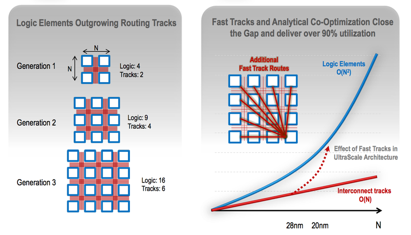
Diagram Xilinx has added 'fast track' routes to try to narrow the gap between logic blocks and routing resource
Peckham said the focus on ASIC-type flows has put more focus on reducing bottlenecks in the routing, particularly for longer-distances connections that frequently take the form of very wide buses, and the clocking mechanisms. “Clock skew becomes more of a problem,” he said.
“With serdes running at up to 28Gbit/s, we have the ability to put enough I/O on the die to get data on and off the chip quickly. The challenge is dealing with that data on the chip. 512bit buses are now quite normal. We have seen 2000bit buses being used,” Peckham noted. “What we’ve done is develop a new capability with fast track routes that run data over longer distances without multiple hops.”
Although the increasing use of wide buses suggests the adoption of bundled wires for routing long-distance connections, “they are not bundled in that they can’t be separated but we have capacity for running multiple signals through the same part of the die,” said Peckham, adding that one of the contributors to skew on FPGAs historically has been the tendency for some parts of the same bus to be split and routed in different directions whereas they would typically be routed together on an ASIC.
Clocking improvements
The Ultrascale architecture changes the way in which clock signals are distributed, using a hierarchical scheme that effectively splits the die into clock tiles. The clock signal for each tile drops into the centre rather than feeding in from the sides, which was typically the case before.
Xilinx has provided the architecture with the ability to power down parts of the FPGA when not in use. “There are some software techniques for switching bits of the FPGA off that aren’t used once we have the bitstream and we switch off memories that are not being used,” said Peckham. “Also, with the Vivado tools we have the capability to do some dynamic power reduction by recognizing when a signal can’t propagate then disabling clocks downstream.”
The previous generation saw Xilinx introduce three types of device, from the high-end Virtex, through the wireless comms-oriented Kintex to the low-cost Spartan follow-on Artix. However, the company considers the 28nm process able to support Artix for the foreseeable future, so will only make UltraScale versions of the Virtex and Kintex. Peckham said the ARM-based Zynq products are likely to see a 20nm upgrade.
“Kintex devices are used in applications such as wireless where memory and digital signal processing are important,” said Peckham.
DSP and memory changes
Xilinx has made a couple of changes to the hardwired multipliers that are provided in dedicated digital signal processing (DSP) blocks, widening them out to 27 x 18bit to better support floating-point algorithms, as well as adding an XOR function.
Although the block RAMs themselves are no bigger than before, the company has added dedicated cascading logic to allow them to be combined more easily. Previously, the cascading needed to be done in programmable logic blocks. Other hard macros being added to the device family include 10/100Gbit/s Ethernet, Interlaken and PCIe. For external memories, the FPGAs will support DDR4.
To help secure designs, the company has increased the depth of AES encryption that can be used to protect the configuration bitstream. “There is a greater focus on design security now,” said Peckham.