Thermal limits challenge Hot Chips power pair
Despite being designed to cut the overall energy consumption of their end applications, two of the custom designs presented at the 26th Hot Chips conference in Cupertino exemplified the problems caused by increasing power density and the benefits of looking at heat removal at the system level.
Adam Butts, research engineer at DE Shaw Research, in describing the philosophy that underpins the team’s highly specialized Anton 2 engine for simulating the ultrafast dynamics of molecular reactions, said: “We are not too concerned about battery life, so we really don’t need to minimize standby power dissipation, which changes our design decisions.”
As the design is meant for carefully controlled data centers, Butts said there was no need to consider temperature excursions. “We have a moderate and well controlled operating temperature, which simpifies those considerations for the design.”
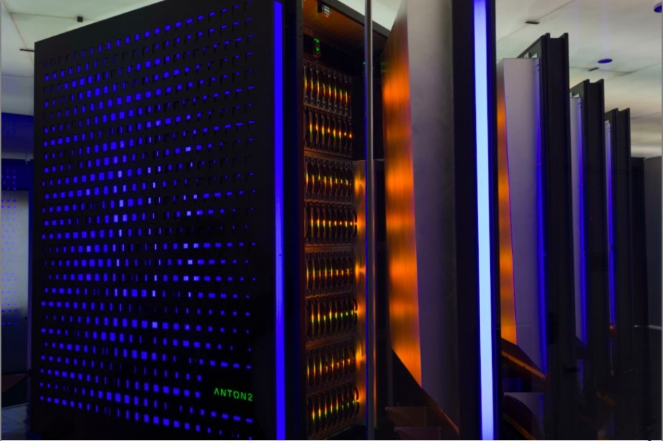
Image Racks at DE Shaw Research containing the Anton 2 ASIC
But with a two billion-transistor, 40nm-process design tuned for throughput – at some 12 tera-operations per second using 32bit arithmetic – the 400mm2 chip still draws a lot of power and produces copious amounts of heat.
Power integrity
“There are a lot of challenges in putting an ASIC of this size together. The main one is power dissipation,” Butts claimed. “That drove a lot of decisions. When you are designing for high power you are concerned with power integrity. The way we dealt with that was with lots and lots of metal. Twenty five per cent of the total metal tracks were used for power delivery. Ninety eight per cent of the allowable metal density of the process’s distribution layer is used for power. And, in total, we have 14,500 core supply bumps [on the package] which makes our die photo look very uninteresting.
“Within the package we had to figure out how to connect the bumps without impacting signal integrity for the serial links. So, there are a lot of decoupling capacitors on the package. Forty percent of the pins on the bottom of the package are core supply balls,” Butts explained, adding that the power and signal planes did not overlap.
Once in the target system, the packaged die is dwarfed by the large copper heatsink and voltage regulator that feeds it power. “The 24-layer circuit board has a lot in it to guarantee power and signal integrity,” said Butts.
For power distribution, the DE Shaw team opted for 48V to improve system energy efficiency. “That’s less of a problem. But heat removal from the system is a problem. We have three large blowers in the rack. And detailed simulations were done to ensure that each node board receives enough air in the rack to keep it cool,” Butts said. Techniques such as adding baffles to the front door helped ensure each slot gets its full share of airflow. Overall, a rack draws 42kW per rack, with some 22kW being supplied to the multiple ASICs.
Butts said the chip taped out December 2012 with the first ASIC powered on April 2013. “The first 512-node segment was operational December 2013 at the lab in New York. We are now working on buildout and performance tuning and we are beginning to use it for actual biochemistry research in-house.”
Mining for money
Another example of a chip with significant thermal challenges, Cointerra’s Goldstrike presents an example of how fast a chip design can be put together and inserted into shipping systems. Cointerra was founded in May 2013 and started shipping its TerraMiner systems to customers in mid-June this year. “There is high pressure to ensure fully functional first silicon,” said Barkatullah, as he described the market for Bitcoin mining.
Since its introduction in 2009, the Bitcoin cryptocurrency has been responsible for focusing compute power on the brute force calculation of SHA256 hashes. To guarantee that Bitcoin transactions cannot be faked – and so prevent counterfeiting – the currency relies on public-key encryption techniques. Buyers and sellers report their private transactions using messages signed by private keys that can be verified using the available public keys.
To ensure that there is a verifiable record of who has valid Bitcoins, the transactions are gathered into blocks and joined with a global ‘blockchain’ – all computers in the network hold a copy. To make it into the blockchain, each block must have a valid hash, which is generated through the process of Bitcoin mining. The hash is signature for that block and, being a hash, even the slightest change to the block’s core data will call for a completely different hash, reducing the probability of a fake hash to near zero. Bitcoin miners receive the currency in exchange for producing valid hashes – they must have a certain number of leading zeroes to qualify. Although the hashes are easy to verify they involve, short of a disruptive improvement to mathematics, a brute-force process of trial and error using the SHA256 algorithm to process.
Compute acceleration
In the early days of Bitcoin, users could expect to generate valid hashes in a matter of minutes on a desktop PC. The algorithm sets the difficulty factor in order to throttle Bitcoin production to a reasonably constant rate. As more computation power arrives on the network, the number of leading zeroes and with them the difficulty factor increases. Algorithms deployed on graphics processing units (GPUs) soon outstripped the ability of desktop PCs to compete profitability – the electricity cost exceeded the value of the Bitcoins mined. Now ASICs tuned purely for SHA256 hash generation have come to dominate the network.
So many tera-operations per second of hash-compute power are being added to the network at the moment that months of delay can render a machine practically useless. The difficulty factor – some 65 leading zeroes – is now so high that even a single TerraMiner machine might not provide a successful result during its lifetime, Timo Hanke, CTO of Cointerra said at Hot Chips.
The machines need to be deployed in bulk to guarantee successful mining, which is why individual miners have formed into collectives that divide up the work and the spoils. Barkatullah said the company has shipped more than 5000 systems so far, representing about 4 per cent of the total processing capacity on the Bitcoin network now.
One unusual aspect of a machine like this is that it needs barely any external I/O – each new input arrives every few seconds. “Our input rate is so low we can afford to use a slow SPI port to transfer data to the GoldStrike chip,” said Barkatullah.
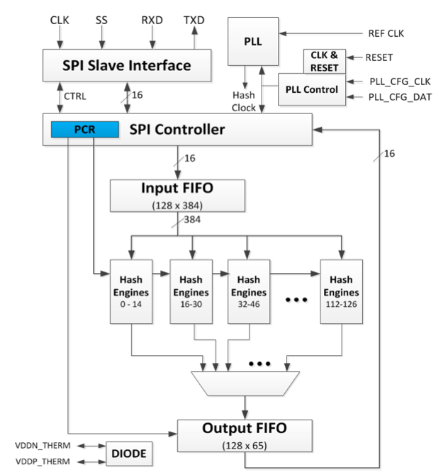
Image Architecture of the Goldstrike ASIC
It’s a different matter inside the chip. Internally, the chip runs at 1GHz, with a central controller determining how values are fed to an array of deep pipelines tuned for hash generation. At any one time, a total of 128 nonce candidates are making their way through the 16 ‘super-pipelines’. To support the clock speed, Cointerra opted for the 28nm HPP process from GlobalFoundries, using nine metal layers. To improve the density of processors in the final system, four chips are put into a single FBGA package.
High-activity logic
The nature of the mining algorithm and the density of the machines presents design issues for mining chips. “You get very high toggle rates,” said Barkatullah. “The SHA algorithm results in toggle rates as high as 80 per cent on some paths, which results in very high power density. So it is a power-to-the-die and cooling challenge.
“At the system level we explored different cooling options. We wanted a common platform for consumers and for data centers. We chose a liquid cooling solution,” said Barkatullah. “A thermal diode monitors the temperature of the hash engines [inside the Goldstrike device].”
Clock distribution presented issues during design, particularly because of the high ratio of sequential logic to combinatorial. “It took several iterations to close timing,” Barkatullah said.
However, the designers were able to take advantage of reuse within the design. “Optimizing the design of the common core blocks paid off big time,” Barkatullah claimed, adding that the combination of in-house designers and contracting out to OpenSilicon achieved “fully functional first silicon in a record amount of time”.
Cointerra is now working on its next generation of Bitcoin-mining ASIC. Barkatullah said: “Our biggest issue is to reduce power density and reduce toggle count. All the things we are doing are proprietary but we are working very hard to reduce the power.”
To try to harness the interest in cryptocurrencies for calculations that have a more beneficial use, Stanford University has launched CureCoin – a conceptual combination of the Folding@Home project and Bitcoin. To demonstrate they have worked hard enough to earn coins, as well as generating hashes, miners have to use processor cycles on their computers to perform protein-folding calculations.
If CureCoin catches on and the economics of mining favor the adoption of ASICs, Anton 2 may provide a preview of what those machines may look like. Although one machine has been donated to the Pittsburgh Supercomputing Center, DE Shaw has up to now only used its custom machine in-house to simulate the atomic interactions of reacting biomolecules, many of them proteins.
Time mismatch
“Biochemistry is an interesting problem. By doing this we can understand more about the internal machinery of the [biological] cell,” Butts claimed.
To do it, Butts said: “Anton 2 uses not just one but two custom processors. Like many physical simulations, molecular dynamics involves cutting up time into discrete segments – in our case, just two femtoseconds long.”
During each time slice, the processors calculate near-neighbor interactions between atoms as well as more distant electrostatic interactions – each of which change the shape, or conformation, of the molecules in the simulated reaction. A lot of the calculations per step are dependent,” said Butts, making it an iterative process which increases runtime.
Standard high-performance computers struggle with the calculations because of the mismatch between the time resolution and the periods of interest DE Shaw’s scientists want to investigate. “Many interesting processing in biology can take time on the order of milliseconds. Having to process 10E12 time steps is not uncommon,” Butts said.
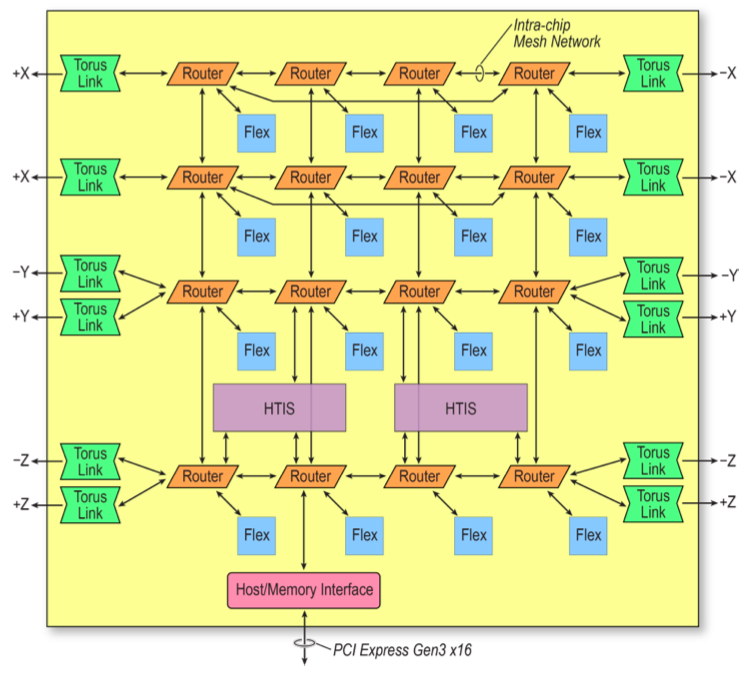
Image The Anton 2 on-chip network and processing units
The bulk of the local interactions take place in what DE Shaw calls the high throughput interaction subsystem – a pipeline of arithmetic units. “Distant interactions and those between bonded atoms happen in the flexible subsystem: so called because its more programmable,” said Butts.
Supporting more than 12 tera-operations per second, the ASIC links to others across six axes, allowing huge three dimensional matrices to be built up using a torus configuration. “This architecture has been a tremendous success for us,” said Butts of Anton 2’s predecessor which introduced the approach at DE Shaw. “It dramatically moved the goalposts for molecular simulation. Anton 2 inherits a lot of that and it does more of it. We now have a lot more compute units. We have a factor of four increase in CPUs and the clock frequency has gotten significantly better. Overall, peak throughput has gone up by a factor of four.”
Regular design
Similar to Goldstrike, Anton 2 employs a tiled design, stepping and repeating the flexible processors in an array across the chip. To preserve die space, the team opted for fixed-point rather than floating-point arithmetic. The effective accuracy of fixed-point arithmetic over the many time steps needed was, Butts said, “a question that we were concerned about with original Anton. The original has shown that it’s not really a problem because the values can be kept fairly well normalized. We get better precision with normalized data than if we used single-precision floating point.”
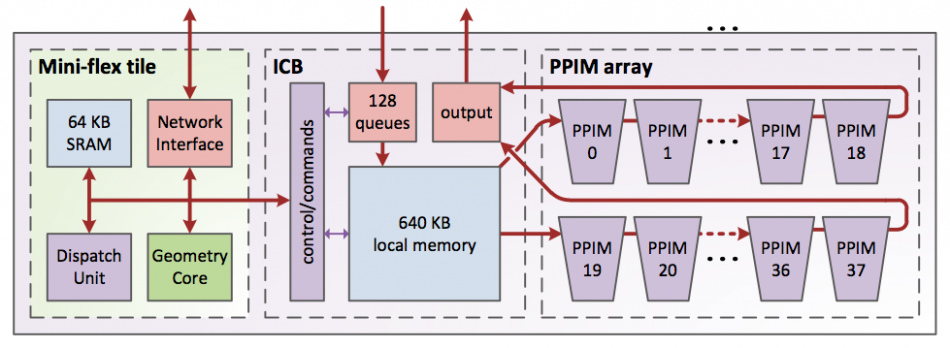
Image Architecture of the HTIS processing unit
A key change compared with the original Anton was a greater alignment in programming terms between the programmable processors in the ASIC. As well as the flexible processors, the high-throughput system has its own management processors. “Originally, we had two different processor cores, which made for a more difficult programming model. These cores converge on a single ISA [instruction set architecture]. We optimized the GCC compiler to target the ISA,” said Butts, as the flexible processors have custom complex instructions used to compute cross products and other matrix-oriented operations.
To support the increase in processing units and clock speed – and the interprocessor communications traffic with those changes – the team moved from using a ring-based on-chip network to a mesh. Butts claimed the aggregate internal bandwidth it supports is “80 per cent of the bandwidth of the internet today”.
The resulting ASIC can compute “a quarter trillion interactions per second”, Butts claimed. Should DE Shaw, founded by a former financial ‘quant’ turn its hand to cryptocurrencies like CureCoin, it will have a massive, albeit expensive head start. However, Butts said the design and verification team for this size of project was “smaller than you might expect” – comprising around 30 people – and the research lab opted for a larger die on an older process which is likely to have reduced non-recurrent engineering costs relative to a project targeting a smaller, possibly higher-yielding die on a 28nm or 20nm process.