TSMC 16nm finFET, Ge 20nm p-finFET set for IEDM
Further details of the TSMC 16nm finFET process will be revealed at the upcoming International Electron Devices Meeting, to be held in Washington DC in December.
The Taiwanese foundry will also detail its continuing work on incorporating germanium in the channel of p-type finFETs to improve mobility.
The 16nm finFET (Guide) process has a 48nm fin pitch and what the company claims is the smallest SRAM ever included in an integrated process – a 128Mbit SRAM measuring 0.07µm2 per bit.
The process offers either, a 35% speed gain or, a 55% power reduction, as compared with TSMC’s existing 28nm HKMG planar process. It has twice the transistor density.
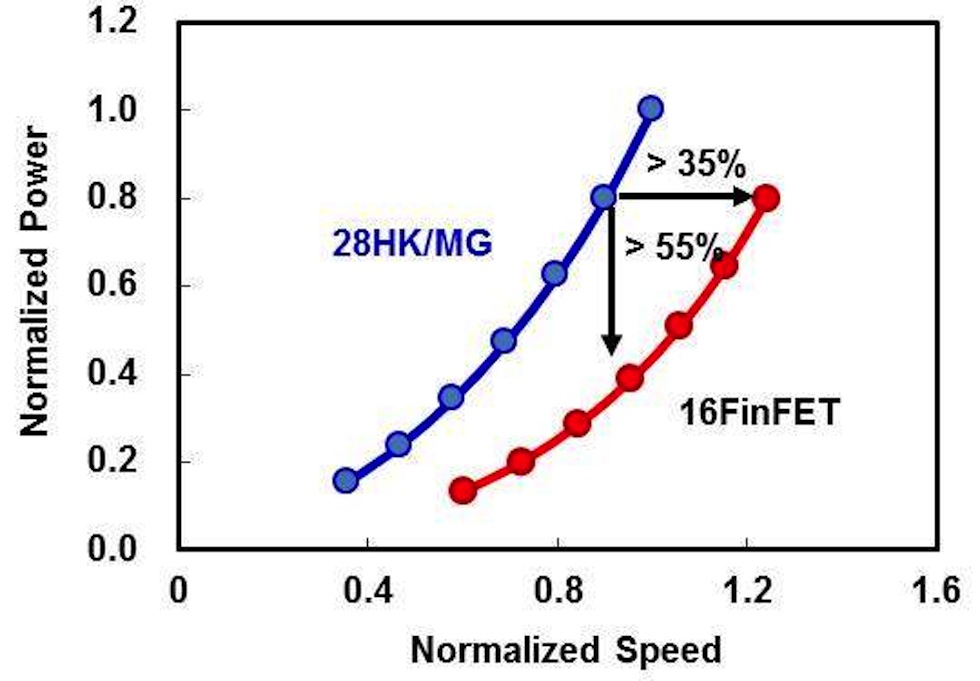
Figure 1 Comparison of the 16nm finFET and 28nm HKMG planar processes (Source: TSMC)
The paper says that short-channel effects are well-controlled in the 16nm process, with DIBL of less than 30 mV/V, saturation current of 520/525A/μm at 0.75V (for NMOS and PMOS, respectively) and off-current of 30pA/μm.
The metal stack incorporates seven levels of high-density copper with low-k interconnect, and high-density planar MIM devices for noise control.
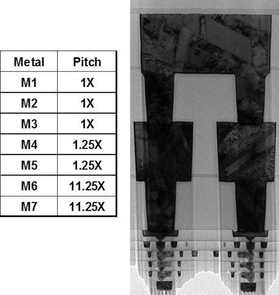
Figure 2 The metal stack of the TSMC 16nm finFET process (Source: TSMC)
(Paper #9.1, “A 16nm CMOS FinFET Technology for Mobile SoC and Computing Applications,” S-Y. Wu et al, TSMC)
Ge 20nm p-finFET
Even as TSMC pushes its mainstream finFET process towards mass production, it is continuing to research enhancements.
Last year we told you about the work TSMC presented at IEDM to integrate germanium into the channel of p-type devices, by using the structure of the device to trap defects resulting from the lattice mismatch caused by growing germanium directly on silicon.
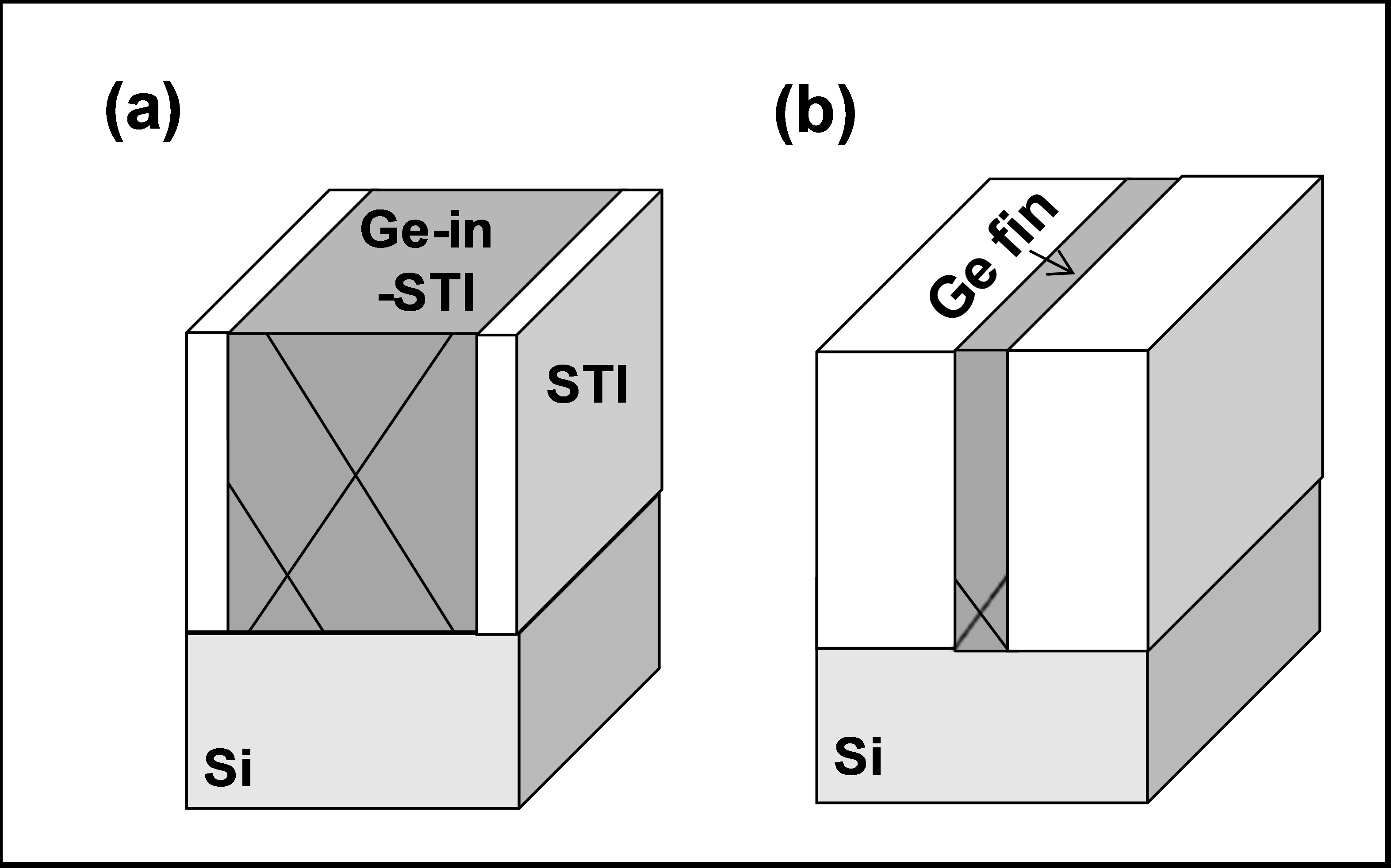
Figure 3 Growing germanium in tall, narrow channels traps defects caused by lattice mismatches with the underlying silicon (Source: TSMC)
This year TSMC will report how it has further improved the performance of these Ge p-channel finFETs by implementing: an optimized 800pm (0.8nm) capacitance-equivalent thickness gate stack made using a replacement-gate process; a scaled-down fin width; and the <110> crystal direction in the channel.
The paper claims that, compared to any other reported non-silicon pFET, the 20nm-channel-length finFETs discussed have demonstrated 2.5 times better subthreshhold slope performance, twice the on/off current and record electrical conductance of 2.7mS/µm.
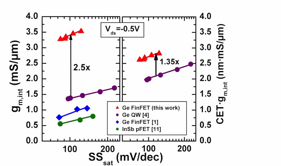
Figure 4 Transconductance gains of using germanium in the channel of p-finFETs (Source: TSMC)
The diagram shows that the transconductance (transport properties) of the p-channel Ge FinFETs is better than any previously reported data at a given subthreshold slope (short channel effects). The right side of the figure then adjusts the transconductance for the difference in gate-oxide thickness, and makes the point that it still shows the advantage over the previous work.
(Paper #20.1, “Scaled P-Channel Ge FinFET With Optimized Gate Stack and Record Performance Integrated on 300mm Si Wafers,” B. Duriez et al, TSMC)
The 59th annual IEEE International Electron Devices Meeting will take place December 9-11, 2013 at the San Francisco Hilton Union Square, preceded by a day of tutorials on Saturday, 7 December and of short courses on Sunday, 8 December.
Find out more here.