Intel, TSMC finFETs to star at IEDM
Intel and TSMC will give further details of their finFET architectures at December’s International Electron Device Meeting in San Francisco.
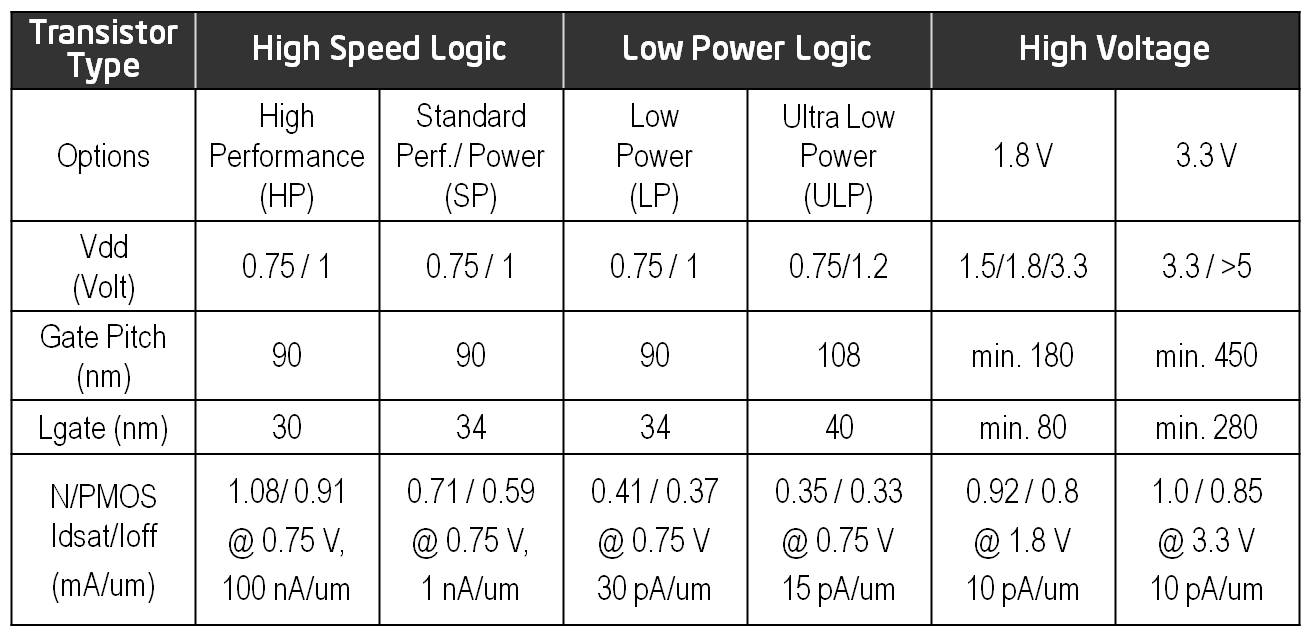
Intel has developed its basic 22nm finFET (Guide) into a suite of devices using multiple gates to give the variety of performance characteristics necessary for SoC designs, including versions offering high speed, low standby power and even tolerance to high voltages.
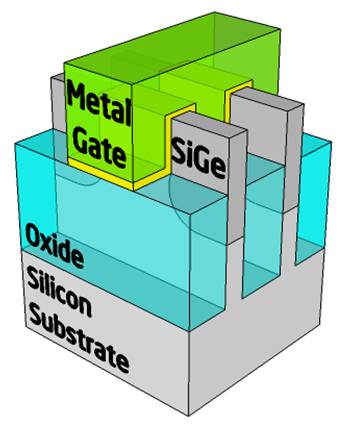
Here’s a look at the basic architectures of two versions of the device, first the high-speed and low-power version:
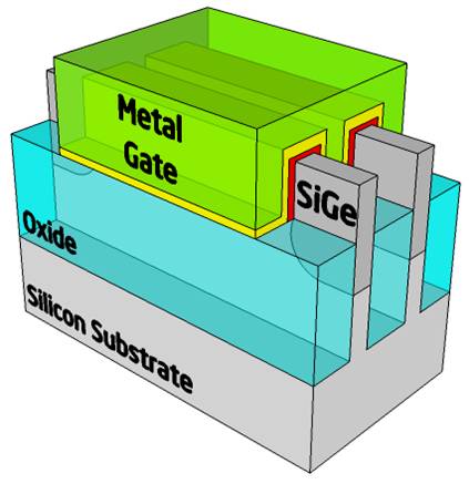
 and then the high-voltage version, with what appears to be an extra layer of insulation over the fin:
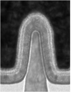
 A look at the fin cross-sections bears this out, with first the high-speed. low-power device:
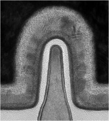
and then the high-voltage device:
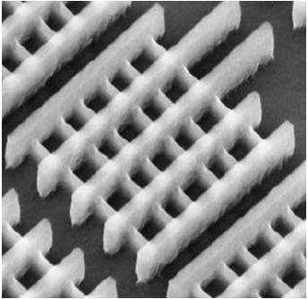
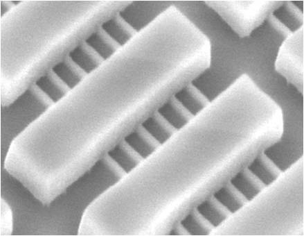
And finally, the traditional aerial SEMs, in the same order as before:
The high-speed logic transistors have subthreshold leakages ranging from 100 nA/µm to 1 nA/µm. The low-power transistors have leakage of less than 50pA/µm yet have drive currents which Intel says are 50% higher than 32nm planar devices. The high-voltage transistors work at 1.8 or 3.3V, to support system I/O standards as well as offering greater headroom for mixed-signal designs such as data converters. Intel says these high voltage transistors have the highest reported I/O device drive currents for an SoC technology (NMOS/PMOS=0.92/0.8 mA/µm at 1.8 V).
The new devices are matched with a new interconnect scheme, with between eight and 11 layers of metallisation with low-k and ultra-low-k dielectrics, and three different SRAM cells, tuned to either high-density/low-leakage (0.092µm2), low voltage (0.108µm2) and high-performance (0.130µm2).
Here’s chapter and verse on the transistors’ performances:
The full details of Intel’s latest work on finFETS will be given in Paper #3.1, “A 22nm SoC Platform Technology Featuring 3-D Tri-Gate and High-k/Metal Gate, Optimized for Ultra-Low-Power, High-Performance and High-Density SoC Applications,” by C.-H. Jan et al, Intel, at the conference.
Meanwhile TSMC has been worrying about improving the p-channel carrier mobility in its finFET design, and has come up with what it says is a simpler way of adding germanium to the fin to achieve this.
The problem to date with introducing germanium into the fin is that the crystal lattices of silicon and germanium don’t match, so if you try to grow the germanium directly on the silicon you get lattice mismatches which cause threading dislocations that grow up into the fin and undermine its performance. The traditional response has been to alloy the two materials at the bottom of the fin to ease the lattice mismatch, and then gradually adjust the concentrations of silicon and germanium in multiple layers so that at the tip of the fin you have pure germanium with a defect-free lattice.
The problem with this approach is that it is slow and therefore costly. TSMC has developed a process which it says enables it to grow the germanium directly on silicon. The trick, apparently, is the geometry of the germanium fin. If you make it relatively tall and narrow, any threading dislocations caused by the lattice mismatch at the interface will quickly terminate in the wall of the fin, rather than growing up into its active region.
Here’s the diagram, showing how threading defects are constrained by the geometry of a tall thin fin:
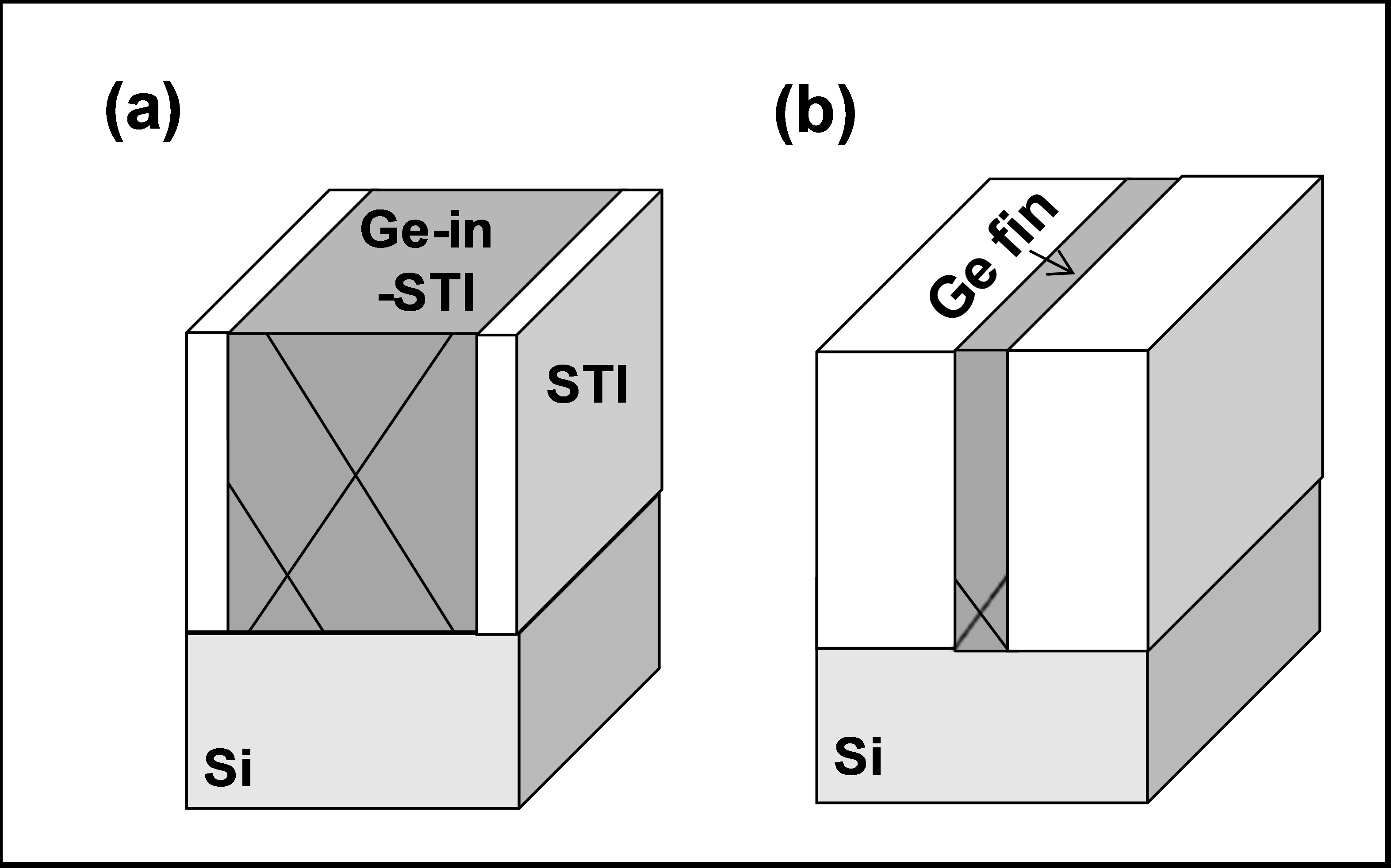
According to the IEDM paper abstract, the key to making this work is to ensure that the fin’s height to width aspect ratio is 1.4 or greater.
TSMC has demonstrated the technique by building devices with good subthreshold characteristics (slope=74mV/dec), good control of short-channel effects, and high performance (1.2mA/µm at Vdd=1V).
There will be full details at IEDM in Paper #23.5, “Demonstration of Scaled Ge P-Channel FinFETs Integrated on Si,” M.J.H. van Dal et al, TSMC.
Discussing improving carrier mobility in finFETs at imec’s International Technology Forum last week, An Steegen, senior vice president of process technology, said that the key to producing a good crystal lattice when there is an abrupt, rather than gradual, change from silicon to germanium is to start with the right (1 1 1) orientation of the silicon substrate, and to ensure that the fin is very narrow – less than 10nm – taking it into the realm of a nanowire.
The 58th annual IEEE International Electron Devices Meeting will take place December 10-12, 2012 at the San Francisco Hilton Union Square, preceded by a full day of short courses on Sunday, Dec. 9 and by a program of 90-minute tutorial sessions on Saturday, Dec. 8.
Find out more here.